当前位置:网站首页>VGA display color bar and picture (FPGA)
VGA display color bar and picture (FPGA)
2022-06-12 13:18:00 【Imperceptible at the beginning】
do as one wishes
One 、VGA agreement
- VGA(Video Graphics Array) Video graphics array is IBM On 1987 A computer display standard using analog signals was proposed in .VGA High resolution 、 The display speed is fast 、 Rich colors, etc .VGA Interfaces are not just CRT Standard interface for display devices , also LCD Standard interface for LCD devices , It has a wide range of applications .
- Principle of use : Display scanning mode is divided into progressive scanning and interlaced scanning : Progressive scanning is scanning from the top left corner of the screen , Point by point from left to right , Every line scanned , The beam returns to the beginning of the next line on the left side of the screen , in the meantime , At the end of each line , Use the line synchronization signal to synchronize ; When all the lines are scanned , Form a frame , Field synchronization with field synchronization signal , And bring the scan back to the top left of the screen , Start the next frame . Interlaced scanning refers to scanning one line every other line during electron beam scanning , After finishing one screen, scan the remaining lines after returning , The interlaced display is flashing so fast , It makes the user's eyes tired . Here we choose the progressive scanning method .
- Please move to the next step for detailed timing relationship
Two 、 Use equipment
The equipment is DE2-115
- TIPS:
Please refer to the development board for the specific implementation method , Like DE2-115 This board , Need to transmit rgb Three primary color data and line field synchronization signal , The transmission clock is also required 、 And blanking signal , And RBG yes 888 The seat is wide , Other boards may be different , You need to change

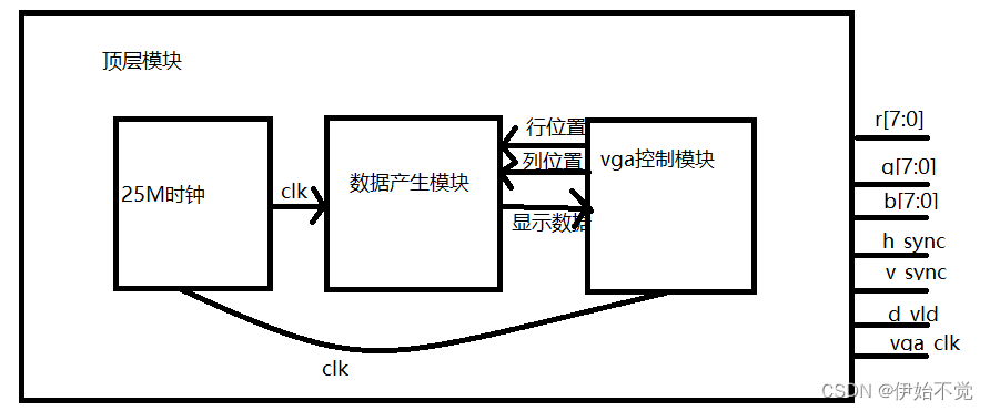
3、 ... and 、 Module design
- The module is divided into clock module 、 Data generation module 、 and vga Control module , The clock module generates the required clock , But it is not automatically set according to the resolution , It's about dying 640*480 @ 60HZ, So for 25M, If you want to write something else , To change the
- The data generation module is based on vga The position transmitted by the control module controls the displayed output , Then output the displayed data back to vga Control module
- vga The control module is the output vga Some control signals of the protocol
Four 、 Code
If a color bar is displayed , You can directly copy the following code , Make the data generation module rom Instantiation and image output comments are OK , Uncomment the output of the color bar output
If the picture is displayed , Need to call rom nucleus , And you need to turn the picture into bmp file , And then bmp To mif file , And then call rom When you change the picture to mif Set file as initialization file , In this way, the address can be read rom Picture data stored in , When the conditions of judgment hold , The picture can be displayed on the display screen .
- counter25M.v:
module counter25M(
  input   wire          clk           , //VGA when
  input   wire          rst_n         , // Reset
  output  reg         clk_25M
);

always @(posedge clk or negedge rst_n) begin
     if (!rst_n) begin
         clk_25M <= 1'b0     ;
     end else  begin
         clk_25M <=  ~clk_25M;
     end
end
endmodule
- data_generate.v:
module data_generate(
 input   wire         clk             , //VGA The clock ,640*480 60hz 25.2MHz
 input   wire         rst_n           , // Reset

 input   wire  [10:0] h_addr           , // Data valid display area , Line address
 input   wire  [10:0] v_addr           , // Data valid display area , Column address
 output  reg  [23:0] data_display       // Display the data
);
wire [23:0] q_sig;// from ip Image data taken from the core
reg  [15:0] address_sig;// Take the address of the picture
wire        pic_area;// Whether it is in the area shown in the picture
parameter PIC_WIDTH = 9'd200;// The picture is long
parameter PIC_HEIGH = 9'd200;// Picture width
parameter BALCK    = 24'h000000,
          RED      = 24'hFF0000,
          GREEN    = 24'h00FF00,
          BLUE     = 24'h0000FF,
          YELLOW   = 24'hFFFF00,
          SKY_BULE = 24'h00FFFF,
          PURPLE   = 24'hFF00FF,
          GRAY     = 24'hC0C0C0,
          WHITE    = 24'hFFFFFF;

// call ip nucleus , Take the data
// The saved picture is 512*512,640*480
rom	rom_inst (
	.address ( address_sig ),
	.clock ( clk ),
	.q ( q_sig )
	);

assign pic_area = h_addr <= PIC_WIDTH && v_addr <= PIC_HEIGH;
// Position change
always @(posedge clk or negedge rst_n) begin
     if (!rst_n) begin
      address_sig <= 16'd0;
     end else if ( address_sig == 40000 ) begin
      address_sig <= 16'd0;
     end else if ( pic_area ) begin// In the display area, it automatically changes with the address change
      address_sig <= h_addr + v_addr * 200 ;
     end
     else begin // Larger than the picture display area , Will keep the address
      address_sig <= address_sig ;
     end
end


// State output , Image output
always @(posedge clk or negedge rst_n) begin
     if (!rst_n) begin
        data_display <= WHITE   ;
     end else begin
        case (pic_area)
            0   : data_display <=   RED           ;
            1   : data_display <=   q_sig         ;
            default: data_display <= data_display ;
        endcase
     end
end

/* // State output , Color bar output
always @(posedge clk or negedge rst_n) begin
     if (!rst_n) begin
        data_display <= WHITE   ;
     end else begin
        case (h_addr)
            0   : data_display <=   BALCK         ;
            80  : data_display <=   RED           ;
            160 : data_display <=   GREEN         ;
            240 : data_display <=   BLUE          ;
            320 : data_display <=   YELLOW        ;
            400 : data_display <=   SKY_BULE      ;
            480 : data_display <=   PURPLE        ;
            560 : data_display <=   GRAY          ;
            default: data_display <= data_display ;
        endcase
     end
end */

endmodule
- vga_contro.v
`define vga_640_480
`include "vga_param.v"


module vga_contro(
 input   wire         clk            , //VGA The clock ,640*480 60hz 25.2MHz
 input   wire         rst_n          , // Reset
 input   wire  [23:0] data_display   , // Display the data

 output  reg   [10:0] h_addr         , // Data valid display area , Line address , Only when it works ,
 output  reg   [10:0] v_addr         , // Data valid display area , Column address
 output  reg           disp_vld      , // Indicates whether the input is valid data , That is, the data in the display area
 output  wire          v_sync        , // Field synchronization signal , One of the conditions for valid data
 output  wire          h_sync        , // Line sync , One of the conditions for valid data , Only when the synchronization signals of row and field are valid , The valid data is entered later
 output  reg   [7:0]   vga_r         , // Red output
 output  reg   [7:0]   vga_g         , // Green output
 output  reg   [7:0]   vga_b         , // Blue output
 output  wire          vga_clk         // Show clock ,
);
parameter H_SYNC_STA = 1;// Line synchronization starts
parameter H_SYNC_END = `H_Sync_Time;// Line synchronization ends
parameter H_DATA_STA = `H_Sync_Time+`H_Right_Border + `H_Front_Porch;// Row data start
parameter H_DATA_END = `H_Sync_Time+`H_Right_Border + `H_Front_Porch + `H_Data_Time;// End of row data

parameter V_SYNC_STA = 1;// Field synchronization starts
parameter V_SYNC_END = `V_Sync_Time;// End of field synchronization
parameter V_DATA_STA = `V_Sync_Time +`V_Bottom_Border + `V_Front_Porch;// Field data start
parameter V_DATA_END = `V_Sync_Time +`V_Bottom_Border + `V_Front_Porch+ `V_Data_Time;// End of field data

reg [(12-1):0] cnt_h; // Count of line addresses
wire add_cnt_h      ; // Line address start flag
wire end_cnt_h      ; // End of line address flag

reg [(12-1):0] cnt_v ; // Count of field addresses
wire add_cnt_v       ; // Field address start flag
wire end_cnt_v       ; // Field address end flag


always @(posedge clk or negedge rst_n) begin
   if (!rst_n) begin
         cnt_h <= 12'b0;
   end else if(add_cnt_h) begin
       if (end_cnt_h) begin
           cnt_h <= 12'b0;
       end else begin
           cnt_h <= cnt_h + 12'b1;
       end
   end
end

assign add_cnt_h = 1'd1;
assign end_cnt_h = add_cnt_h && cnt_h == `H_Total_Time - 1;


always @(posedge clk or negedge rst_n) begin
   if (!rst_n) begin
         cnt_v <= 12'b0;
   end else if(add_cnt_v) begin
       if (end_cnt_v) begin
           cnt_v <= 12'b0;
       end else begin
           cnt_v <= cnt_v + 12'b1;
       end
   end
end

assign add_cnt_v = end_cnt_h;
assign end_cnt_v = add_cnt_v && cnt_v == `V_Total_Time - 1;


// Synchronous signal
assign  h_sync = (cnt_h > ( H_SYNC_STA - 1) && cnt_h < (H_SYNC_END - 1) );
assign  v_sync = (cnt_v >= ( V_SYNC_STA - 1) && cnt_v <= (V_SYNC_END - 1) );

assign vga_clk = ~clk;


// Define a valid display area
always @(posedge clk or negedge rst_n) begin
     if (!rst_n) begin
        h_addr <=  11'd0;
     end else if(cnt_h >= (H_DATA_STA - 1) && cnt_h <= (H_DATA_END - 1)) begin
        h_addr <=  cnt_h - (H_DATA_STA - 1);
     end else begin
        h_addr <=  11'd0;
     end
end

// Define a valid display area
always @(posedge clk or negedge rst_n) begin
     if (!rst_n) begin
        v_addr <=  11'd0;
     end else if(cnt_v >= (V_DATA_STA - 1) && cnt_v <= (V_DATA_END - 1)) begin
        v_addr <=  cnt_v - (V_DATA_STA - 1);
     end else begin
        v_addr <=  11'd0;
     end
end


// Valid area output
always @(posedge clk or negedge rst_n) begin
     if (!rst_n) begin
        vga_r <= 8'd0  ;
        vga_g <= 8'd0  ;
        vga_b <= 8'd0  ;
        disp_vld <= 1'b0;
        // Output when data is valid
     end else if(cnt_h >= (H_DATA_STA - 1) && cnt_h <= (H_DATA_END - 1) && cnt_v >= (V_DATA_STA - 1) && cnt_v <= (V_DATA_END - 1)) begin
        vga_r <= data_display[23-:8]  ;
        vga_g <= data_display[15-:8]  ;
        vga_b <= data_display[07-:8]  ;
        disp_vld <= 1'b1 ;
     end else begin
        vga_r <= 8'd0 ;
        vga_r <= 8'd0 ;
        vga_r <= 8'd0 ;
        disp_vld <= 1'b0 ;
     end
end


endmodule
- vga_param.v:
//`define vga_480_272
`define vga_640_480
//`define vga_800_480
//`define vga_800_600
//`define vga_1024_600
//`define vga_1024_768
//`define vga_1280_720
//`define vga_1920_1080

`ifdef vga_480_272
      `define H_Right_Border  0
	`define H_Front_Porch   2
	`define H_Sync_Time     41
	`define H_Back_Porch    2
	`define H_Left_Border   0
	`define H_Data_Time     480
	`define H_Total_Time    525

	`define V_Bottom_Border 0
	`define V_Front_Porch   2
	`define V_Sync_Time     10
	`define V_Back_Porch    2
	`define V_Top_Border    0
	`define V_Data_Time     272
	`define V_Total_Time    286

`elsif vga_640_480
      `define H_Right_Border  8
	`define H_Front_Porch   8
	`define H_Sync_Time     96
	`define H_Back_Porch    40
	`define H_Left_Border   8
	`define H_Data_Time     640
      `define H_Total_Time    800

      `define V_Bottom_Border  8
      `define V_Front_Porch   2
      `define V_Sync_Time     2
	`define V_Back_Porch    25
	`define V_Top_Border    8
      `define V_Data_Time     480
      `define V_Total_Time    525

`elsif vga_800_480
      `define H_Right_Border  0
      `define H_Front_Porch   40
      `define H_Sync_Time     128
      `define H_Back_Porch    88
      `define H_Left_Border   0
      `define H_Data_Time     800
      `define H_Total_Time    1056

	`define V_Bottom_Border 8
	`define V_Front_Porch   2
	`define V_Sync_Time     2
	`define V_Back_Porch    25
	`define V_Top_Border    8
	`define V_Data_Time     480
	`define V_Total_Time    525

`elsif vga_800_600
      `define H_Right_Border  0
      `define H_Front_Porch   40
      `define H_Sync_Time     128
      `define H_Back_Porch    88
      `define H_Left_Border   0
      `define H_Data_Time     800
      `define H_Total_Time    1056

      `define V_Bottom_Border 0
      `define V_Front_Porch   1
      `define V_Sync_Time     4
      `define V_Back_Porch    23
      `define V_Top_Border    0
      `define V_Data_Time     600
      `define V_Total_Time    628


`elsif vga_1024_600
      `define H_Right_Border   0
      `define H_Front_Porch    24
      `define H_Sync_Time      136
      `define H_Back_Porch     160
      `define H_Left_Border    0
      `define H_Data_Time      1024
      `define H_Total_Time     1344

      `define V_Bottom_Border  0
      `define V_Front_Porch    1
      `define V_Sync_Time      4
      `define V_Back_Porch     23
      `define V_Top_Border     0
      `define V_Data_Time      600
      `define V_Total_Time     628

`elsif vga_1024_768
      `define H_Right_Border   0
      `define H_Front_Porch    24
      `define H_Sync_Time      136
      `define H_Back_Porch     160
      `define H_Left_Border    0
      `define H_Data_Time      1024
      `define H_Total_Time     1344

      `define V_Bottom_Border  0
      `define V_Front_Porch    3
      `define V_Sync_Time      6
      `define V_Back_Porch     29
      `define V_Top_Border     0
      `define V_Data_Time      768
      `define V_Total_Time     806

`elsif vga_1280_720
      `define H_Right_Border   0
      `define H_Front_Porch    110
      `define H_Sync_Time      40
      `define H_Back_Porch     220
      `define H_Left_Border    0
      `define H_Data_Time      1280
      `define H_Total_Time     1650

      `define V_Bottom_Border  0
      `define V_Front_Porch    5
      `define V_Sync_Time      5
      `define V_Back_Porch     20
      `define V_Top_Border     0
      `define V_Data_Time      720
      `define V_Total_Time     750

`elsif vga_1920_1080
     `define H_Right_Border  0
     `define H_Front_Porch   88
     `define H_Sync_Time     44
     `define H_Back_Porch    148
     `define H_Left_Border   0
     `define H_Data_Time     1920
     `define H_Total_Time    2200

     `define V_Bottom_Border 0
     `define V_Front_Porch   4
     `define V_Sync_Time     5
     `define V_Back_Porch    36
     `define V_Top_Border    0
     `define V_Data_Time     1080
     `define V_Total_Time    1125

`endif
- vga_protocol_top.v
module vga_protocol_top(
 input   wire          clk           , //VGA The clock ,640*480 60hz 25.2MHz
 input   wire          rst_n         , // Reset
 output  wire          v_sync        , // Field synchronization signal
 output  wire          h_sync        , // Line sync
 output  wire   [7:0]  vga_r         , // Red output
 output  wire          disp_vld       , // Whether it is time to display
 output  wire   [7:0]  vga_g         , // Green output
 output  wire   [7:0]  vga_b         , // Blue output
 output  wire          vga_clk         // Show clock ,
);

wire  [23:0] data_display;
wire  [10:0] h_addr      ;
wire  [10:0] v_addr      ;
counter25M u_counter25M(
    .clk      ( clk      ),
    .rst_n    ( rst_n    ),
    .clk_25M  ( clk_25M  )
);

vga_contro u_vga_contro(
    .clk           ( clk_25M       ),
    .rst_n         ( rst_n         ),
    .data_display  ( data_display  ),
    .h_addr        ( h_addr        ),
    .v_addr        ( v_addr        ),
    .disp_vld      (disp_vld       ),
    .v_sync        ( v_sync        ),
    .h_sync        ( h_sync        ),
    .vga_r         ( vga_r         ),
    .vga_g         ( vga_g         ),
    .vga_b         ( vga_b         ),
    .vga_clk       ( vga_clk       )
);


data_generate u_data_generate(
    .clk     ( clk_25M ),
    .rst_n   ( rst_n   ),
    .h_addr  ( h_addr  ),
    .v_addr  ( v_addr  ),
    .data_display  ( data_display  )
);

endmodule
- gitee : vga_protocol
- Coloured ribbon

- picture

5、 ... and 、 summary
- vga The agreement looks complicated at first sight , But it is not complicated after understanding , The row field synchronization signal is the sign of the beginning of each row or column , The function of the blanking signal is to indicate that the following data is valid data , It is not difficult to understand the timing , Data filling is just like dot matrix .
边栏推荐
- "New continent" of mobile application going to sea
- Itk:: neighborhood get 6 neighborhood, 18 neighborhood, 26 neighborhood, 18/6 neighborhood, 26/18 neighborhood
- import torch_geometric 加载一些常见数据集
- 达梦数据库DM8 windows环境安装
- [cloud native | kubernetes] in depth understanding of deployment (VIII)
- [embedded] serial communication and its case
- Getting started with NVIDIA Jetson nano Developer Kit
- torch_geometric mini batch 的那些事
- How to adapt the page size when iframe is embedded in a web page
- R语言ggplot2可视化:使用ggrepel包在线图(line plot)的尾端那个数据点添加数值标签(number label)
猜你喜欢

How to balance multiple losses in deep learning?

Volume mount and mirror creation

入门深度学习与机器学习的经验和学习路径

Image comparison function after registration itk:: checkerboardimagefilter

It is enough to read this article. Web Chinese development

Freshman girls' nonsense programming is popular! Those who understand programming are tied with Q after reading
![[you code, I fix] whitesource was officially renamed mend](/img/0f/75ac1d0b08244ed689733d38551a61.jpg)
[you code, I fix] whitesource was officially renamed mend

Microsoft Word 教程,如何在 Word 中插入页眉或页脚?

Innovation training (x) advanced interface beautification

镜像扫描工具预研
随机推荐
Share PDF HD version, series
Script引入CDN链接提示net::ERR_FILE_NOT_FOUND问题
[cloud native | kubernetes] in depth understanding of deployment (VIII)
Redis消息队列重复消费问题
itkMultiResolutionImageRegistrationMethod
Volume mount and mirror creation
移动应用出海的“新大陆”
Chrome debugging tool
创新实训(十一)开发过程中的一些bug汇总
[brush title] probability of winning a draw
jsp跳转问题,不能显示数据库数据,并且不能跳转
JVM 运行时参数
Microsoft Word tutorial, how to insert a header or footer in word?
在 Debian 10 上独立安装MySQL数据库
【云原生 | Kubernetes篇】深入了解Deployment(八)
Successful job hopping Ali, advanced learning
Newoj week 10 question solution
import torch_geometric 的Data 查看
Getting to know blob objects
Redis message queue repeated consumption