当前位置:网站首页>Hardware development notes (III): basic process of hardware development, making a USB to RS232 module (II): design principle diagram Library
Hardware development notes (III): basic process of hardware development, making a USB to RS232 module (II): design principle diagram Library
2022-06-21 23:30:00 【Changsha Red fatty QT】
If the article is original , Reprint please indicate the source of the original
This article blog address :https://hpzwl.blog.csdn.net/article/details/124913345
Red fat man ( Red Imitation ) The complete blog of : Development technology collection ( contain Qt Practical technology 、 Raspberry pie 、 The three dimensional 、OpenCV、OpenGL、ffmpeg、OSG、 Single chip microcomputer 、 The combination of software and hardware and so on ) Ongoing update …( Click on the portal )
Hardware related development
Last one :《 Hardware development notes ( Two ): Basic process of hardware development , To make a USB turn RS232 Module ( One ): Basic development process and component selection 》
Next :《 Hardware development notes ( Four ): Basic process of hardware development , To make a USB turn RS232 Module ( 3、 ... and ): Schematic design 》
Preface
In the previous article, I learned about the basic process , Relevant chips are selected , This chapter describes the design process of schematic diagram , Before or in the process of schematic design, it is necessary to continuously add schematic elements and devices .
Allegro、OrCad
Cadence The company aims at PCB Aspect EDA Products can be roughly divided into high-end and low-end , High end is Cadence SPB, The low end is OrCAD.
No matter high-end or low-end , The schematic part is mainly purchased OrCAD Schematic software in ( It's called Capture).
PCB The drawing is different , High-end Cadence SPB It's called Allegro, Low-end OrCAD Now it mainly uses Allegro A simplified version of the , Will contain the complete PSpice( Circuit simulation software ).
OrCad Design schematic library
When designing the schematic diagram , It is necessary to establish the basic identification graphics of components , Some come with them , Some are provided by the government or suppliers , There are also , We choose to build our own ( Mainly describe the process ).
Step one : start-up OrCad

( Be careful : yes Capture CIS, No separate Cadence OrCad Icon ).
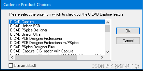


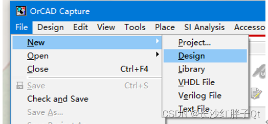
Step two : New project usbTtlRs232


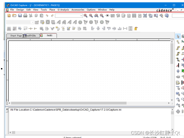
Step three : Adjust the window layout
Adjust the window distribution :


Maybe the software is old , Didn't like VS That kind of automatic layout , When the main window is zoomed , The child window will not be scaled :
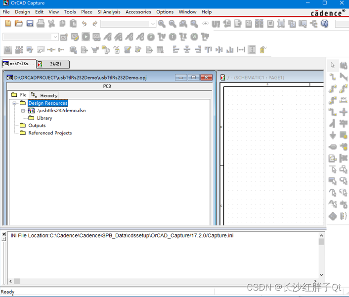
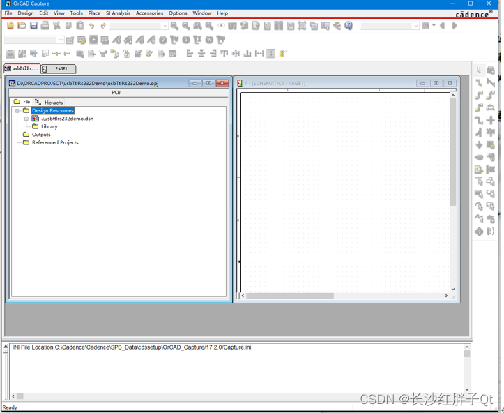
Manual adjustment :


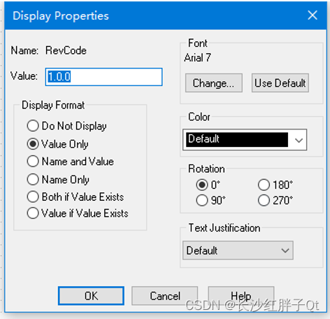
Step four : Modify properties and versions

Double click the pop-up attribute box to modify :

Change the version number :

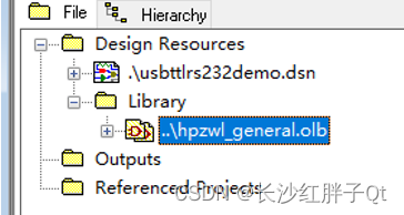
Step five : Library file import
OrCad I brought some libraries with me , In the installation directory :


Library description view :《 Hardware practical skills :OrCad Built in schematic diagram olb/OLB Introduction to library enumeration 》
Common components , I like to build my own database .
Step six : Establish schematic Library
( Delete the introduced ).
Has generated :

Modify name :

Modified :
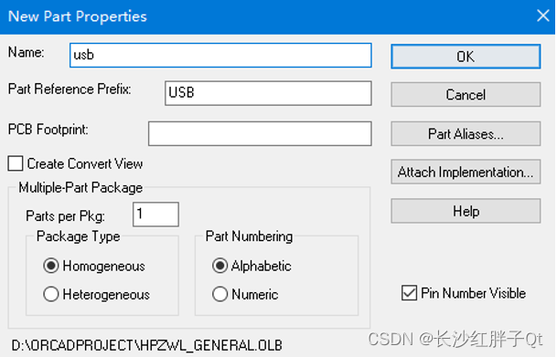
Step seven : Add new components and place
USB( Male head )
On the schematic diagram , You can choose to show it , You can also choose not to be obvious , Finally, the schematic diagram is needed lib And pcb Of lib For pin mapping decisions .


The tools are as follows :


Select schematic , Then place the components :


ASM1117


2.54mm DIP

CH340G
Typical circuits recommended in the manual :

Pins not drawn , All are suspended by default :

MAX232
Refer to the circuit diagram on the screenshot of the manual above to draw :

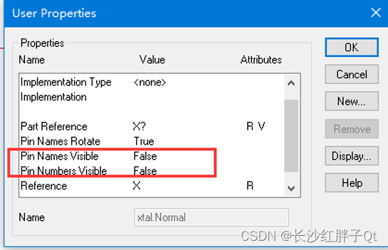
Crystal oscillator


Step eight : All schematic libraries are placed on the schematic


Last one :《 Hardware development notes ( Two ): Basic process of hardware development , To make a USB turn RS232 Module ( One ): Basic development process and component selection 》
Next :《 Hardware development notes ( Four ): Basic process of hardware development , To make a USB turn RS232 Module ( 3、 ... and ): Schematic design 》
边栏推荐
- Precautions for using keep alive
- uniapp版本更新 热更新及自然更新
- Matplotlib drawing and displaying Chinese
- 解决笔记本电脑(i)某个键的字母按不出来
- 硬件开发笔记(五):硬件开发基本流程,制作一个USB转RS232的模块(四):创建CON连接器件封装并关联原理图元器件
- keep-alive的使用注意点
- 使用云开发实现微信支付的具体方法
- How to associate the QR code of wechat applet and realize the integration of two codes
- #CISSP认证2021年教材 OSG 第9版 增(改)知识点:与 第8版 的目录对比
- UniApp之播放视频、 下载视频到手机相册、添加下载进度条功能(踩坑记录)
猜你喜欢

Some users of uniapp wechat authorization cannot be authorized normally

H5之微信授权登陆 (uniapp网页版微信授权登录)

你有一个机会,这里有一个舞台

libra白皮书

If you spend 200W to buy traffic, it is better to start at 0 cost and make an independent station with high private domain operation income!

Sigir2022 𞓜 user preference modeling in conversational recommendation system

Multi order MFCC extraction for speech signal processing (matlab)

Speech breakpoint detection (short time improved subband spectral entropy)
uni-app进阶之样式框架/生产环境【day10】

Solution to garbled Chinese display of securefx transmission remote server

随机推荐
Precautions for using keep alive
Translation software Bob installation tutorial
关于 SecureFx传输远程服务器中文显示乱码 的解决方法
阿里出品!图形化的ant脚本——IDEA插件CloudToolkit
盘点常见的漏洞利用方式
[understanding pointer] advanced level of pointer
Uniapp version update hot update and natural update
[wustctf2020] plain and unpretentious -1
树莓派开发笔记(十七):树莓派4B+上Qt多用户连接操作Mysql数据库同步(单条数据悲观锁)
Jupyter lab cannot be used after installing the extension
Use of three values of pointer events
开发环境和测试环境的发包(及uniapp的request封装)
About the solution to the "fatal error: gl/gl.h: no such file or directory" of Qilin system development error
今日睡眠质量记录81分
【用四道刁钻例题带你理解】数据在内存中存储的方式
Uniapp encapsulates the request function to achieve unique login. One account can only log in to one device at the same time
Flink实战之实时风控规则引擎
泰山OFFICE技术讲座:微软雅黑字体故意设置的坑,粗体错误
pointer-events的三个值的使用
Flink real-time risk control rule engine