当前位置:网站首页>PWM (pulse width modulation) of STM32 notes
PWM (pulse width modulation) of STM32 notes
2022-06-21 12:13:00 【Summer foam and light rain】
Write it at the front :
The purpose of this article is to summarize backup 、 For future reference , Because it's a personal summary , If there is any wrong , Welcome to correct ; in addition , Most of the content comes from the Internet 、 Books 、 And all kinds of manuals , In case of infringement, please inform , Immediately delete the post and apologize .
Catalog
Two 、STM32F1 Chinese vs PWM Support for
6、 ... and 、 And PWM Regulation related functions
7、 ... and 、 Routine demonstration
One 、PWM brief introduction
Pulse width modulation ( English :Pulse Width Modulation, abbreviation :PWM), abbreviation Pulse width modulation , It is a technology that converts analog signals into pulses , Generally, the period of the converted pulse is fixed , But the working period of the pulse will change according to the size of the analog signal .
Usually we use it a lot PWM Technology is used to adjust light or speed , This is also the most common .
Two 、STM32F1 Chinese vs PWM Support for
stay STM32F1 Inside ,PWM The generation of is by Timer Output , But not all of them Timer All support ; Be careful , What we are talking about here is the use of hardware technology to produce PWM, It produces PWM The frequency is very considerable , As for software timing control IO Output pin , The so-called software PWM technology , I won't elaborate here .
Learn from the above ,STM32F1 Of Timer Can produce PWM Of , But not all of them Timer All support ; therefore , Look through the manual , It can be learned that , Support PWM Hardware output technology Timer Yes “ Universal timer ” and “ Advanced control timing ” These two types , And for “ Basic timer ” No PWM Hardware output technology , So we should pay a little attention in practical application , So as not to cause unreasonable resource allocation .
1、 Universal timer (TIM2 ~ TIM5)

Every time there is 4 Independent channels as output :

2、 Advanced control timer (TIM1 & TIM8)

This timer can generate 7 road PWM Output :

3、 Basic timer (TIM6 & TIM7)

Explanation of timer , You can read the previous chapter :STM32 Note it Timer( Timer )
3、 ... and 、PWM Count mode
- Edge alignment mode
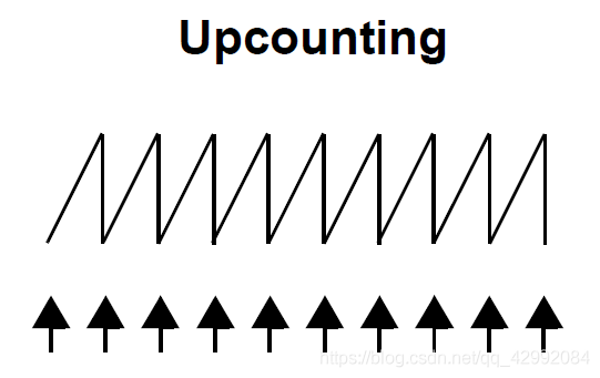
1、 Count up
2、 Count down

- Center alignment mode

Four 、 working principle
Take counting up as an example :
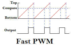
The count value is fixed from... Per cycle Bottom Start counting , I've been tired Top, Then count again ; As long as it doesn't stop running , So it goes back and forth ; from Bottom Add up to Top For a cycle , In order to make PWM pulse , And all we have to do is set up Compare Value , thus , Just one more Compare reference value , It can also be called split value ; When counting , Count every time you accumulate , All follow Compare Comparison of values , When the count value is equal to Compare Value at the same time , The control output state is the opposite , So as to get the Output Plot line of .
5、 ... and 、PWM Output mode
above-mentioned ,Compare Comparison of values , When the count value is equal to Compare Value at the same time , The control output state is the opposite ; therefore , There will be two duty cycle states , One is when the figure above Compare To Top The output is high level , The other is the opposite Bottom to Compare High level between .
So that corresponds to STM32 in , Its status is determined in TIMx_CCMRx Register bit 6:4 Of OCxM[2:0] in :

Be careful :STM32 Medium PWM The mode just distinguishes when the active level is , However, it is not determined whether the high level is active or the low level is active . This needs to be combined CCER The register of CCxP Bit to determine .
6、 ... and 、 And PWM Regulation related functions
| function | function |
void TIM_SetClockDivision(TIM_TypeDef* TIMx, uint16_t TIM_CKD) | Clock division factor setting |
void TIM_PrescalerConfig(TIM_TypeDef* TIMx, uint16_t Prescaler, uint16_t TIM_PSCReloadMode) | TIM_x Prescaler setting |
void TIM_SetAutoreload(TIM_TypeDef* TIMx, uint16_t Autoreload) | Set the automatic loading cycle of the timer |
void TIM_SetCompare1(TIM_TypeDef* TIMx, uint16_t Compare1) | Set the comparison value of each channel ( It can be understood as duty cycle ) |
void TIM_SetCompare2(TIM_TypeDef* TIMx, uint16_t Compare2) | |
void TIM_SetCompare3(TIM_TypeDef* TIMx, uint16_t Compare3) | |
void TIM_SetCompare4(TIM_TypeDef* TIMx, uint16_t Compare4) |
Generally speaking , Calculate what you need PWM frequency = System clock / Clock division factor / TIM_x prescale / Automatic loading cycle .
7、 ... and 、 Routine demonstration
Let's say TIM3 Of ch3、4 As an example :
#define TIME3_ARR			624			//  Automatic reload register cycle value
#define TIME3_PSC			71			// TIMx Clock frequency prescaled value
#define TIME3_PULSE			(uint16_t)((TIME3_ARR+1) / 2 - 1)		//  Compare register values

#define TIME3_CH3_PIN       GPIO_Pin_0
#define TIME3_CH4_PIN       GPIO_Pin_1

uint16_t Time3_CCR3_Val = TIME3_PULSE;
uint16_t Time3_CCR4_Val = TIME3_PULSE;

void TIM3_PWM_Init(void)
{
    GPIO_InitTypeDef GPIO_InitStructure;
    TIM_TimeBaseInitTypeDef  TIM_TimeBaseStructure;
    TIM_OCInitTypeDef  TIM_OCInitStructure;

    RCC_APB1PeriphClockCmd(RCC_APB1Periph_TIM3, ENABLE);
    RCC_APB2PeriphClockCmd(RCC_APB2Periph_GPIOB | RCC_APB2Periph_AFIO, ENABLE);
    GPIO_InitStructure.GPIO_Pin = TIME3_CH3_PIN | TIME3_CH4_PIN;
    GPIO_InitStructure.GPIO_Mode = GPIO_Mode_AF_PP;
    GPIO_InitStructure.GPIO_Speed = GPIO_Speed_50MHz;
    GPIO_Init(GPIOB, &GPIO_InitStructure);				// IO Mouth configuration

    /* Time base configuration */
    TIM_TimeBaseStructure.TIM_Period = TIME3_ARR;
    TIM_TimeBaseStructure.TIM_Prescaler = TIME3_PSC;	// 1600Hz
    TIM_TimeBaseStructure.TIM_ClockDivision = TIM_CKD_DIV1;        //  Clock division factor
    TIM_TimeBaseStructure.TIM_CounterMode = TIM_CounterMode_Up;
    TIM_TimeBaseInit(TIM3, &TIM_TimeBaseStructure);		//  Basic configuration of timer

    /* PWM1 Mode configuration: Channel3 */
    TIM_OCInitStructure.TIM_OCMode = TIM_OCMode_PWM1;   // PWM mode 1
    TIM_OCInitStructure.TIM_OutputState = TIM_OutputState_Enable;
    TIM_OCInitStructure.TIM_Pulse = Time3_CCR3_Val;     //  Duty cycle setting
    TIM_OCInitStructure.TIM_OCPolarity = TIM_OCPolarity_High;    //  Polarity is high

    TIM_OC3Init(TIM3, &TIM_OCInitStructure);

    TIM_OC3PreloadConfig(TIM3, TIM_OCPreload_Enable);

    /* PWM1 Mode configuration: Channel4 */
    TIM_OCInitStructure.TIM_OutputState = TIM_OutputState_Enable;
    TIM_OCInitStructure.TIM_Pulse = Time3_CCR4_Val;

    TIM_OC4Init(TIM3, &TIM_OCInitStructure);

    TIM_OC4PreloadConfig(TIM3, TIM_OCPreload_Enable); //  Enable pre loading ( Can make  CCR4 Preload of )

    TIM_ARRPreloadConfig(TIM3, ENABLE); //  Enable automatic reloading of registers  ARR Preload of

    /* TIM3 enable counter */
    TIM_Cmd(TIM3, ENABLE);
}
ad locum , Pay attention to TIM_ARRPreloadConfig() function , Its function is only to allow or prohibit the timer to ARR Whether to update immediately after writing the new value in the buffer of , The operation is TIMx->CR1 Medium “APRE” position , Its bit is explained as follows :

We can't get any useful information from the above explanation , You need to combine the following two examples to understand :
chart 1:APRE = 0( The default value is ), When ARR When the value is modified , At the same time, update the value of shadow register immediately

You can see that the previous parameter is ARR = FF, When ARR Reassign to zero 36 after , It will take effect immediately , And is equal to 36 Overflow occurred at , And generate an event .
chart 2:APRE = 1, When ARR When the value is modified , It has to be in the next event UEV The value of the shadow register cannot be updated until it occurs
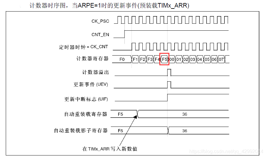
You can see here that the previous parameter is ARR = F5, When to modify ARR The value of is 36, Only the reload register value of the surface has changed , But the shadow register that really works doesn't change . At this time, you need to wait until the end of the previous cycle , An update event occurred , The shadow register will be modified .
And in the program ,TIM_ARRPreloadConfig(TIM3, ENABLE); So that when we change the value , Avoid triggering events that do not conform to the parameters before and after modification during switching ( In the picture above 2 For example , If it is not enabled APRE, So here you are ARR Reassign to zero 36 after , The data will take effect immediately ; Because we were counting at that time F1 It was modified when , meanwhile , because APRE = 0, So when we count to F5 It will not generate an event and reset the count value ( At this time, the trigger value becomes 36 了 ), Will run until 0xFFFF( With 16bit Take the timer as an example ) Then the register overflows again 0 Start counting , Finally, I counted to 36 An event occurs when , Then it will cause , The total count during this switch is : 0xFFFF - 0x00F5 + 36; If in PWM In mode , In this way, it becomes writing new ARR When the value of , It is possible to generate a high when switching ( low ) Irregular pulses of level ( It does not conform to the requirements before and after modification )).
alike , about TIM_OCxPreloadConfig() The same goes for functions .
8、 ... and 、 other
1、 It is worth noting that , Using advanced timer TIM8 When ( Maybe other advanced timers need to be added , But in TIM1 Has been opened by default ), Need to add again TIM_CtrlPWMOutputs(TIM8, ENABLE); Execute the function to output PWM wave . in the light of TIM_CtrlPWMOutputs function , See the following instructions :
/**
  * @brief  Enables or disables the TIM peripheral Main Outputs.
  * @param  TIMx: where x can be 1, 8, 15, 16 or 17 to select the TIMx peripheral.
  * @param  NewState: new state of the TIM peripheral Main Outputs.
  *   This parameter can be: ENABLE or DISABLE.
  * @retval None
  */
void TIM_CtrlPWMOutputs(TIM_TypeDef* TIMx, FunctionalState NewState);
2、 For using Keil Software simulation , Use the built-in logic analyzer to see the waveform , You have to set the clock frequency :

Then you need to set it here ( Remember to go back to your chip ):
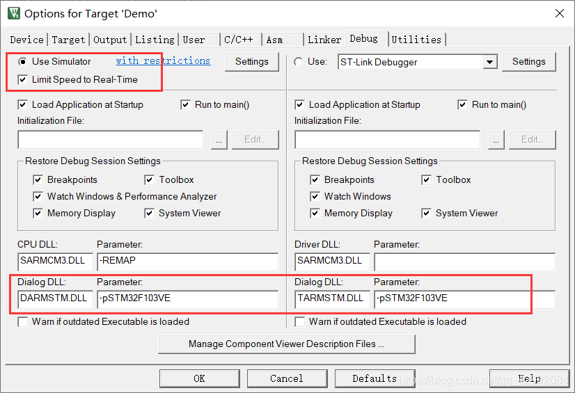
And then go into DEBUG Pattern , Set up PWM Output port ( There is a random one here ):

Last , The key is coming. :Keil Software waveform simulation , Relatively a little unreliable , Do not use this if you can observe with an oscilloscope , Or get a logic analyzer , also , As if Keil Does not support TIM5 Observe the above timer output .
边栏推荐
猜你喜欢

uniapp中常用到的方法(部分) - 时间戳问题及富文本解析图片问题

i.MX - RT1052 脉宽调制(PWM)

Snow Ice City (blackened)

知识点:PCB电路板的几种特殊布线方法

i.MX - RT1052输入输出(GPIO)

【无标题】

MySQL 5.6.49 企业版设置密码复杂度策略

RPC(远程过程调用协议)

南京大学 静态软件分析(static program analyzes)-- Intermediate Representation 学习笔记
![[cloud native | Devops] Jenkins installation and actual combat (II)](/img/1f/68ec217a920fb7c737227137e3243c.png)
[cloud native | Devops] Jenkins installation and actual combat (II)
随机推荐
Codeworks round 797 (Div. 3) F. shifting string problem solution
The k-th small__
harmonyos培训一
External attention tensorflow (under update)
PCB电路板设计都有哪些注意事项?
Redis里5种基本数据类型常用指令
STM32开发之 VS Code + GDB下载调试
What are the precautions for PCB design?
External-Attention-tensorflow(更新中)
The final battle of the giant: instant retailing
6-zabbix monitors and automatically discovers the memory and CPU usage of third-party Middleware
Use huggingface to quickly load pre training models and datasets in the moment pool cloud
创建型模式 - 单例模式
findpanel的相关代码
看懂UML类图和时序图
MySQL-DDL
Anchor of SSD_ Box calculation
6-Zabbix监控自动发现第三方中间件内存及CPU使用情况
广东发产品检测券,消费者也有份
i.MX - RT1052输入输出(GPIO)