当前位置:网站首页>Full process flow of CMOS chip manufacturing
Full process flow of CMOS chip manufacturing
2022-07-29 07:18:00 【Luca cat】
Details of the whole process of chip manufacturing

Chip generally refers to the carrier of integrated circuit , It's also an integrated circuit that has been designed 、 manufacture 、 encapsulation 、 The results of the test , It's usually a separate whole that can be used immediately . If you put the CPU CPU It's like the heart of the whole computer system , So the chipset on the motherboard is the trunk of the whole body . For the motherboard , The chipset almost determines the function of the motherboard , And then affect the performance of the entire computer system , Chipset is the soul of motherboard .
So if you want to build a chip , First , You have to draw something like this for Foundry ( Outsourcing wafer manufacturing companies )▼

Zoom in ▼

We finally see a gate circuit ! This is a NAND Gate( NAND gate ), Something like that ▼

A, B It's input , Y It's output
The blue one is metal 1 layer , Green is metal 2 layer , Purple is metal 3 layer , Pink is metal 4 layer . The transistor (“ The transistor ” since 199X Since then, it has been mainly MOSFET, That's field effect control ) Well ? Look at the picture carefully , See those white dots inside ? That's the substrate , And some green borders ? Those are Active Layer ( That is, doping layer ).
Foundry How does it work ? It can be divided into the following steps :
First of all, we got a wafer of silicon , ( It's a big piece of crystalline silicon , It's very smooth , It's usually round )
The pictures are arranged according to the production steps . But the step summary is written separately .
1、 Wet washing ( Keep silicon wafer surface free of impurities with various reagents )
2、 Photolith ( Irradiate silicon wafers with ultraviolet light through the mask , It's easy to wash out where you're being photographed , Leave the place untouched as it is . So you can carve the desired pattern on silicon wafers . Be careful , No impurities have been added at this time , It's still a silicon wafer . )
3、 Ion implantation ( Different impurities are added at different positions in the silicon wafer , Different impurities depend on the concentration of / Different positions make up the FET .)
4.1、 Dry etching ( There are many shapes that we didn't need before , It's etched for ion implantation . Now we're going to wash them off with plasma , Or some structures that don't need to be engraved in the first step of lithography , This step is etching ).
4.2、 Wet etching ( Wash away further , But with reagents , So it's called wet etching )—— After the above steps are completed , Field effect transistor has been made , But the above steps are usually done more than once , It's likely to need to be done over and over again , To meet the requirements .
5、 Plasma washing ( Bombard the whole chip with a weaker plasma beam )
6、 heat treatment , Which is divided into :
6.1 Rapid thermal annealing ( It's to flash the whole film through a high-power light 1200 Above centigrade , And then slowly cool down , In order to make the implanted ions better start-up and thermal oxidation )
6.2 Anneal
6.3 Thermal oxidation ( Making silicon dioxide , The gate of the FET (gate) )
7、 Chemical vapor deposition (CVD), Further refinement of the various substances on the surface
8、 Physical vapor deposition (PVD), similar , And you can add coating
9、 Molecular beam epitaxy (MBE) If you need long single crystals, you need .
10、 Electroplating
11、 chemical / Mechanical surface treatment
12、 Wafer testing
13、 Wafer grinding can be factory packaged .
Then look step by step through the diagram ▼

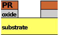
1、 There's an oxide layer on it , Here's the substrate ( silicon )—— Wet washing

2、 Generally speaking , First, inject a small amount of (10^10 ~ 10^13 / cm^3) Of P Type of substance ( One electron is missing from the outermost layer ), As a substrate —— Ion implantation

3、 Join first Photo-resist, Protect where you don't want to be etched —— Photolith
4、 Top mask ! ( It's the label Cr The place of . Empty in the middle means no cover , Black means covered up .) —— Photolith

5、 UV light up , The one below is reflected —— Photolith

6、 Remove the mask —— Photolith
7、 Wash away the exposed oxide layer , Exposing the silicon layer ( You can inject ions )—— Photolith

8、 Remove the protective layer . So you get a silicon wafer ready to be injected . This step is repeated over and over again on silicon ( Dozens or even hundreds of times )—— Photolith

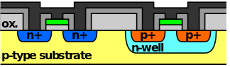
9、 And then after lithography , Insert a small amount of (10^14 ~ 10^16 /cm^3) Injected N A type of substance makes a N-well (N- well )—— Ion implantation

10、 Dry etch the need for P-well It's also etched out , You can also use lithography again —— Dry etching
11、 The picture above will P- A thin layer of silicon dioxide is oxidized again from the top of the A-type semiconductor —— heat treatment
12、 A layer of polycrystalline silicon grown by molecular beam epitaxy , This layer can conduct electricity —— Molecular beam epitaxy
13、 Further etching , Make fine structures .( In annealing and part of CVD)—— repeat 3-8 Photolith + Wet etching
14、 Again, insert a lot of (10^18 ~ 10^20 / cm^3) Injected P/N Type of substance , Note that at this time MOSFET Has been basically formed —— Ion implantation

15、 Accumulate in gas phase The nitride layer formed —— Chemical vapor deposition

16、 Etch the nitride out of the channel —— Photolith + Wet etching
17、 Physical vapor deposition produces Metal layer —— Physical vapor deposition

18、 Etch the excess metal layer . Photolith + Wet etch repeat 17-18 Every layer of metal grows .
The steps of the attached drawings are marked at the bottom of each figure , altogether 18 Step .
The final shape is about this :

among , step 1-15 Belong to Front-end processing (FEOL), That is, how to do the appearance effect tube . step 16-18 ( Plus a lot of repetition ) It belongs to back-end processing (BEOL), The back-end wiring is mainly used to process . In the beginning, all we could see in the big chip was wiring ! In general, the underlying silicon can hardly be seen on a highly concentrated chip , Will be covered by wiring .
SOI (Silicon-on-Insulator) technology :
Tradition CMOS The drawback of technology is : The thickness of the substrate affects the parasitic capacitance on the chip , Indirectly leads to the performance degradation of the chip . SOI Technology is mainly about making Source pole / Drain electrode and The silicon substrate separates , In order to achieve ( part ) The purpose of eliminating parasitic capacitance .
Tradition :

SOI:

The main production methods are as follows ( It's mainly about making silicon - silicon dioxide - The structure of silicon , The following steps are basically the same as the traditional process .)
1. High temperature oxidation annealing :

A layer of oxygen ion is implanted on the surface of silicon

Oxygen ions penetrate into the silicon layer , Forming an oxygen rich layer

High temperature annealing

forming
Or is it
2. Wafer Bonding( Use two ! ) Don't you want to make a sandwich structure ? I don't need money ! Two yuan, please !


For silicon 2 Surface oxidation

For silicon 2 Hydrogen ion implantation of silicon 2 Hydrogen ion implantation

Turn over

The hydrogen ion layer is treated as a bubble layer, and the hydrogen ion layer is treated as a bubble layer

Cut off the excess. Cut off the excess
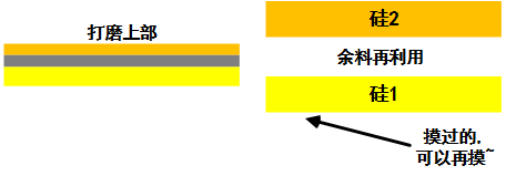
forming + recycling

Photolith

Ion implantation ion implantation
The length of the micro graph is like this :

Lithography again + etching

Remove protection , The middle one is Fin Remove protection , The middle one is Fin

Polysilicon at the gate / high K Polysilicon at the gate of dielectric growth / high K Medium growth

The growth of the oxide layer at the gate

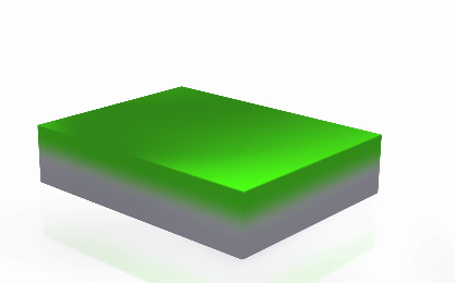
Grow up like this

Source pole Drain fabrication ( Photolith + Ion implantation )

Primary metal / Polysilicon patch

etching + forming

Physical vapor deposition produces a surface metal layer ( Because it's a three-dimensional structure , All connections should be made at the top )

Mechanical polishing ( Yes ! Not grinding will lead to inconsistent thickness of the metal layer )

forming ! forming !

边栏推荐
- [Charles' daily problems] when you open Charles, you can't use nails
- Kubernetes (五) ---------部署 Kubernetes Dashboard
- 微服务远程调用
- MySQL 高级(进阶) SQL 语句 (一)
- 1172. The plate stack has a sequence table + stack
- SSH password free login - two virtual machines establish password free channel two-way trust
- JS 鸡生蛋与蛋生鸡问题,Object与Function究竟谁出现的更早?Function算不算Function的实例?
- buck电路boot和ph引脚实测
- CMOS芯片制造全工艺流程
- 【C语言刷LeetCode】67. 二进制求和(E)
猜你喜欢


随机推荐
Improved pillar with fine grained feature for 3D object detection paper notes
Nodejs安装教程
【charles日常问题】开启charles,使用不了钉钉
Flink实时仓库-DWD层(交易域-加购维度退化处理)模板代码
[C language brush leetcode] 2332. The latest time to get on the bus (m)
Interface test actual project 03: execute test cases
Hj37 statistics of the total number of rabbits per month Fibonacci series
做开发4年13K,想转行自动化测试,薪资还能涨吗···
Homebrew brew update doesn't respond for a long time (or stuck in updating homebrew...)
Revolution of game assets
gin 服务退出
SpingBoot整合Quartz框架实现动态定时任务(支持实时增删改查任务)
WPF嵌套布局案例
Pod基本介绍
时钟树综合(一)
聊天机器人有何用处?有何类型?看完这些就明白了!
OCR光学字符识别方法汇总
Vscode remote debugging PHP solution through remotessh and Xdebug
Tp6 use protobuf
JS chicken laying eggs and egg laying chickens. Who appeared earlier, object or function? Is function an instance of function?