当前位置:网站首页>PCB layout must know: teach you to correctly lay out the circuit board of the op amp
PCB layout must know: teach you to correctly lay out the circuit board of the op amp
2022-08-05 10:18:00 【Ji Ke Lao Bai】
In the circuit design process, application engineers often overlook the layout of the printed circuit board (PCB).The problem often encountered is that the schematic of the circuit is correct, but it doesn't work, or just runs at low performance.
In this article, a great engineer will show you how to properly lay out an op amp's circuit board to ensure its functionality, performance, and robustness.
Incident Replay
Engineers and their intern designed with an OPA191 op amp in a non-inverting configuration with a gain of 2V/V, a load of 10k, and a supply voltage of +/-15V.Figure 1 shows a schematic of the design.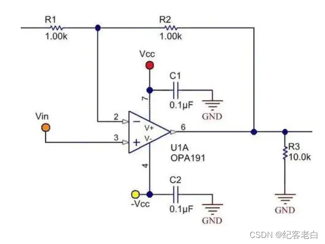
Figure 1 OPA191 schematic in non-inverting configuration
The engineer assigns the intern to lay out the board for this design and gives him general guidance on PCB layout (ie, keep the board trace paths as short as possible, while keeping the components close together to reduce the size of the boardspace) and let him design it himself.
How difficult is the design process?It's really just a few resistors and capacitors, isn't it?
Figure 2 shows the layout of the interns' first attempt at designing.The red line is the path for the top layer of the board, while the blue line is the path for the bottom layer.![[image]](/img/52/2241495f834f3926c0a37c377efd7c.png)
Figure 2 First Layout Attempt Scheme
Realized CircuitThe board layout wasn't as intuitive as I thought it would be, and the engineer felt that there should be some more detailed instructions for the interns.The intern followed his advice exactly when designing, shortening the traces and placing the components closely together.But this layout can be further improved to reduce board parasitic impedance and optimize its performance.
The first improvement they made was to move resistors R1 and R2 next to the inverting pin (pin 2) of the OPA191; this helped reduce stray capacitance on the inverting pin.
The inverting pin of an op amp is a high impedance node and therefore has high sensitivity.Longer trace paths can act as wires, allowing high frequency noise to couple into the signal chain.PCB capacitance on the inverting pin can cause stability problems.Therefore, the contact on the inverting pin should be as small as possible.
Moving R1 and R2 next to pin 2 allows the load resistor R3 to be rotated 180 degrees, which brings decoupling capacitor C1 closer to the positive supply pin (pin 7) of the OPA191.It is extremely important to place the decoupling capacitors as close as possible to the supply pins.Longer trace paths between the decoupling capacitors and the power supply pins increase the inductance of the supply pins, which reduces performance.
Another improvement they made is the second decoupling capacitor C2.The via connection of VCC to C2 should not be placed between the capacitor and the power supply pins, but should be routed where the supply voltage must pass through the capacitors to the power supply pins of the device.
Figure 3 shows how to move each part and vias to improve the layout.![[image]](/img/6c/e42ad51abf393da7c2e81993b80e44.png)
Figure 3 The position of each component to improve the layout
You can addWide trace paths to reduce inductance, which is equivalent to the size of the pads that the trace paths connect to.It can also flood the ground planes on the top and bottom layers of the board, creating a solid, low-impedance path for return current.Figure 4 shows the final layout.![[image]](/img/c5/545fc7509306be4b4c1b3a39757a1c.png)
Figure 4 Final layout----
边栏推荐
- 开发常用手册链接分享
- static linking and dynamic linking
- PHP operation mangoDb
- 一个栈的输入序列为1 2 3 4 5 的出站顺序的理解
- SQL外连接之交集、并集、差集查询
- mysql索引
- Bias lock/light lock/heavy lock lock is healthier. How is locking and unlocking accomplished?
- FPGA:基础入门按键控制LED灯
- 5. Deploy the web project to the cloud server
- Huawei's lightweight neural network architecture GhostNet has been upgraded again, and G-GhostNet (IJCV22) has shown its talents on the GPU
猜你喜欢

What is CRM Decision Analysis Management?

Create a Dapp, why choose Polkadot?
dotnet OpenXML parsing PPT charts Getting started with area charts
Meteorological data processing example - matlab string cutting matching and R language date matching (data splicing)
【AGC】增长服务1-远程配置示例
教你本地编译运行一个IDEA插件,在IDEA里聊天、下棋、斗地主!

E-sports, convenience, efficiency, security, key words for OriginOS functions
阿里全新推出:微服务突击手册,把所有操作都写出来了PDF

three.js debugging tool dat.gui use

Oracle temporary table space role
随机推荐
【AGC】增长服务1-远程配置示例
高质量 DeFi 应用构建指南,助力开发者玩转 DeFi Summer
开发常用手册链接分享
技术干货 | 基于 MindSpore 实现图像分割之豪斯多夫距离
The founder of the DFINITY Foundation talks about the ups and downs of the bear market, and where should DeFi projects go?
牛刀小试基本语法,Go lang1.18入门精炼教程,由白丁入鸿儒,go lang基本语法和变量的使用EP02
FPGA:基础入门按键控制LED灯
The difference between find, matches, lookingAt matching strings in matcher
【Unity】【UGUI】【在屏幕上显示文本】
你最隐秘的性格在哪?
Bias lock/light lock/heavy lock lock is healthier. How is locking and unlocking accomplished?
Is digital transformation a business buy-in?
MySQL之数据视图
第九章:activit内置用户组设计与组任务分配和IdentityService接口的使用
单片机:温度控制DS18B20
three.js debugging tool dat.gui use
Can MySQL use aggregate functions without GROUP BY?
Ali's new launch: Microservices Assault Manual, all operations are written out in PDF
Common operations of oracle under linux and daily accumulation of knowledge points (functions, timed tasks)
Score interview (1)----related to business