当前位置:网站首页>Quartus call & design D trigger Simulation & timing wave verification
Quartus call & design D trigger Simulation & timing wave verification
2022-06-23 13:37:00 【Little monster】
quartus call & Design D trigger —— Simulation & Time series wave verification
Catalog
1、 stay Quartus-II I use the gate circuit to design a D trigger , And simulate , Timing waveform verification ;
2、 stay Quartus-II Directly call a D Trigger circuit , Conduct simulation , Timing waveform verification , And 2 compare ;
3、 stay Quartus-II use Verilog Write a language D trigger , Conduct simulation verification
One 、 know D trigger
D A trigger is a device with memory function , Information storage device with two stable states , Is to constitute a variety of
The most basic logic unit of a sequential circuit, It is also an important unit circuit in digital logic circuit .
D Trigger inClock pulses CP The leading edge of the ( Positive jump 0→1) Flipping occurs, The secondary state of the trigger depends on CP Before the rising edge of the pulse arrives D The state of the end , namelySubstate =D. therefore , It has 0、 Set up 1 Two functions . Because in CP=1 During this period, the circuit has the function of maintaining blocking , So in CP=1 period ,D The data state of the terminal changes , It will not affect the output state of the trigger .
D Triggers are widely used , It can be used as the deposit of digital signals , Shift deposit , Frequency division and waveform generator, etc .
1、 structure
D trigger (data flip-flop or delay flip-flop) from 4 A NAND gate , among G1 and G2 Constitute the basic RS trigger . When the level triggered master-slave trigger works , The input signal must be added before the positive jump edge . If in CP Interference signal appears at the input during high level , Then it is possible to make the trigger state error . The edge trigger allows you to CP The trigger edge comes to the moment before adding the input signal . such , The time when the input is disturbed is greatly shortened , The possibility of interference is reduced . edge D Triggers are also called sustain - Blocking edges D trigger . edge D The trigger can consist of two D The trigger is connected in series , But the first one D Trigger CP Need to use non gate reverse .
2、 features
Menu 
Sequence diagram 
This is right D A brief introduction to triggers , For more D Understanding of triggers , You can refer to the following link ;
D trigger .
Two 、 Design D Trigger timing verification
1、 Create a project
file—>new project wizard
Edit project name , Click later next
Choose the right chip and its family 
direct next
Project creation complete , Click on finish
2、 Create a box file
Click on new
Select the signature in the red box 
Select... As shown 
choice nand2, Two input NAND gates , Add... In turn 4 individual nand2 And a non gate not
After adding, as shown in the figure 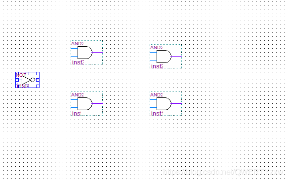
Select the connection tool 
The wiring effect is shown in the figure ( Double click the mouse to change the pin name )
Save the circuit diagram 
3、 Compile schematic file
Compile the circuit diagram 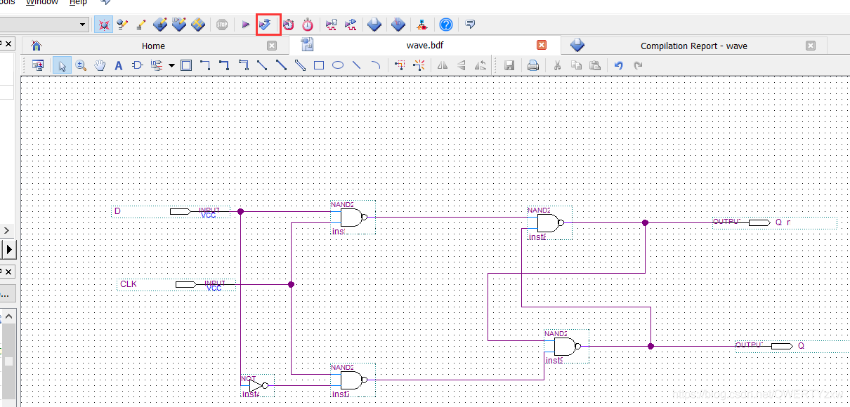
Compiler interface 
rtl viewer, Check the hardware circuit diagram 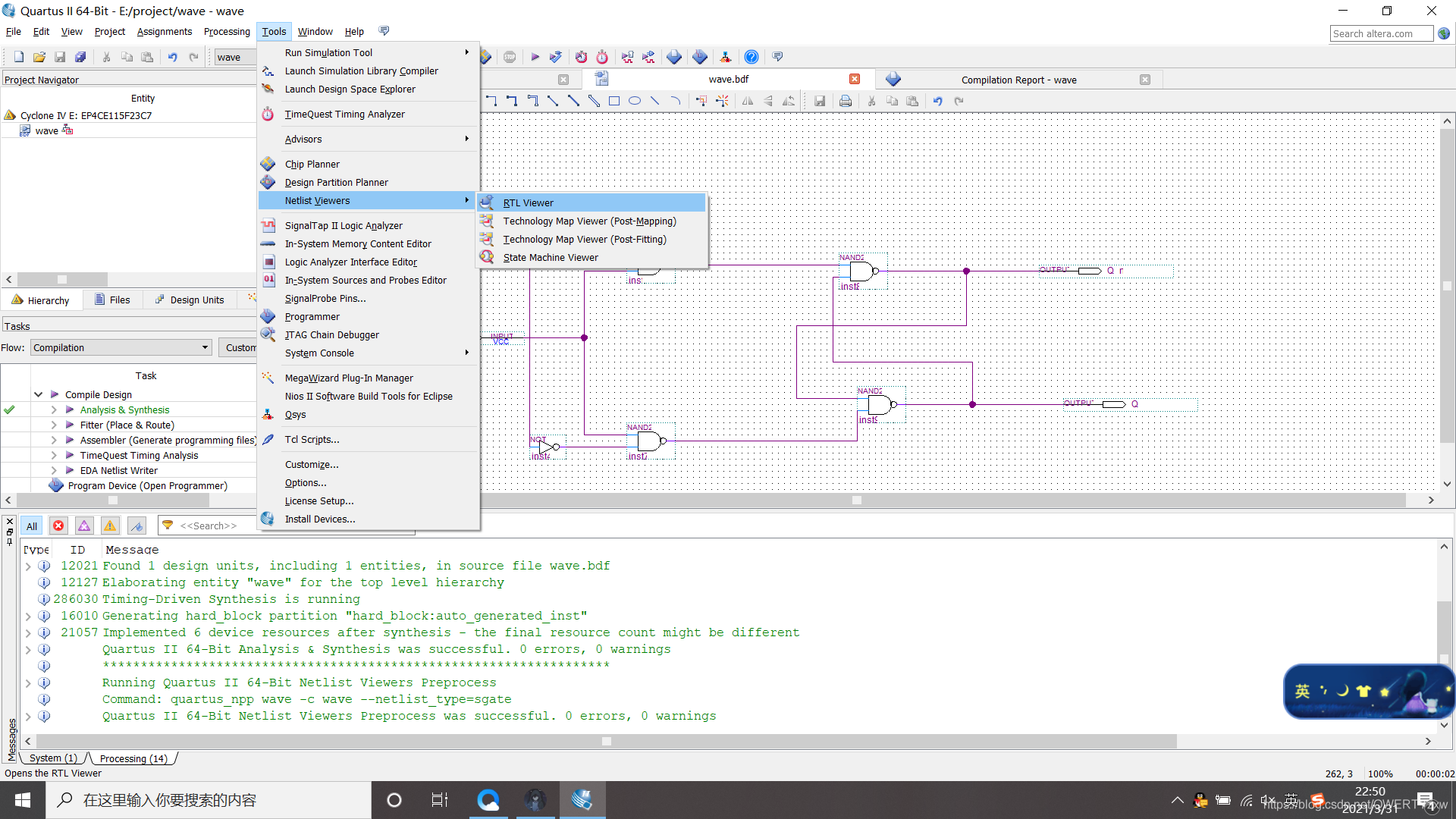
Circuit diagram 
4、 establish vwm Waveform file
Select the icon vwm
Operation as shown in figure 
add to node or bus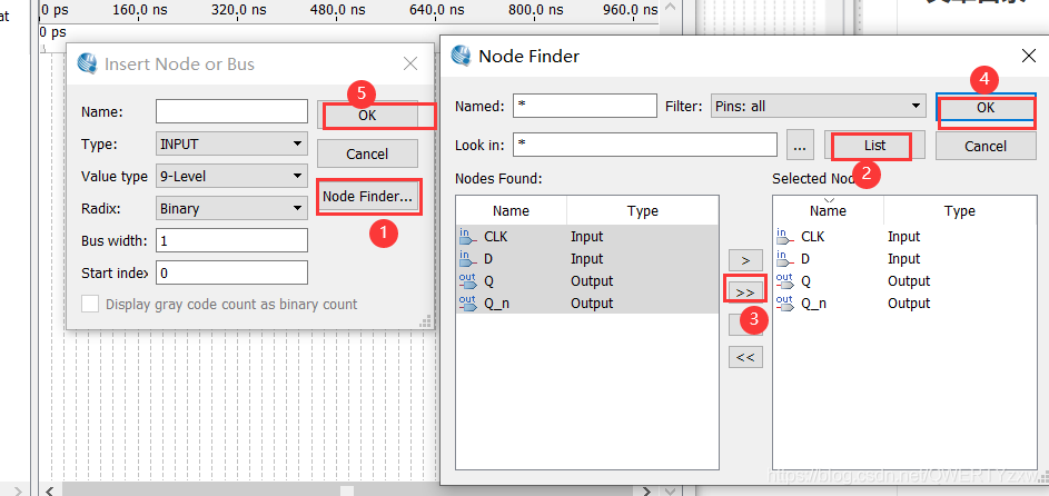
Effect display 
Edit input signal clk, Generate a clock signal 
Mouse selection D,Q The signal Q_n, Editing ( Select with the left mouse button Double click to change the value )
5、 Timing waveform simulation
compile 
There is an error 
Connect modelsim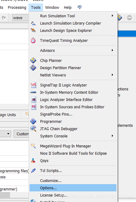
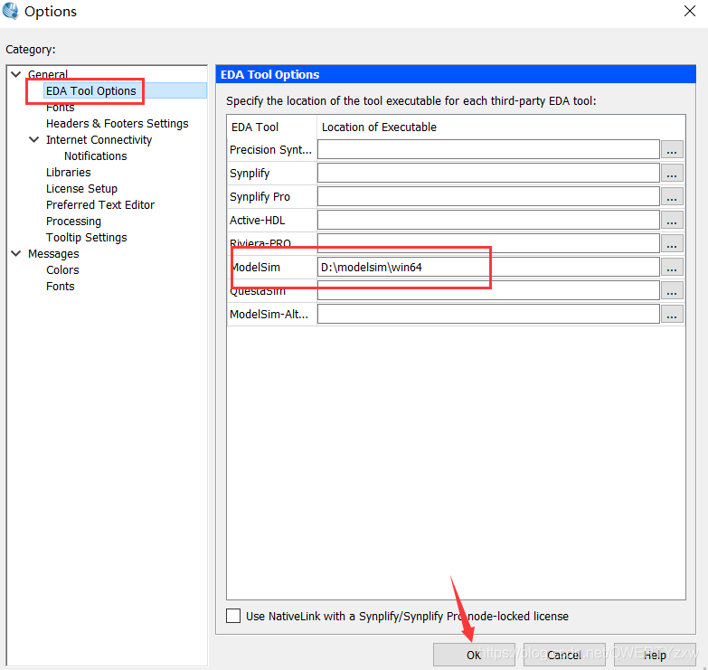
Error reporting solution 
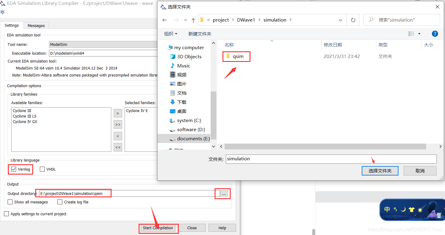
The result is shown in Fig. 
Simulation results 
3、 ... and 、 call D Trigger timing verification
1、 Create a box file
The creation method is the same as above
call D trigger 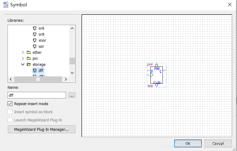
Wiring patch pin , The effect is as shown in the picture (Ctrl+ The mouse wheel can zoom the trigger pin, etc )
2、 Compile the schematic
Check the hardware diagram 
compile 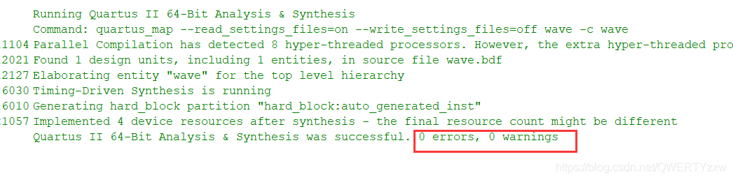
3、 establish vwm Waveform file and simulation
wave form 
Timing simulation results 
Four 、verilog Language implementation D Trigger timing verification
1、 To write verilog file
Create the project first , Method is the same as above.
establish Verilog file , Click on file—new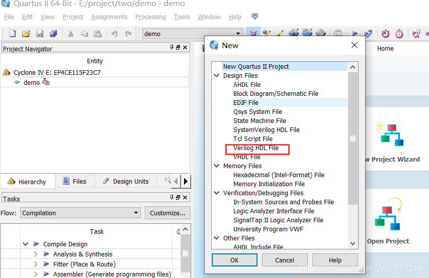
Paste the following code
//demo File name
module demo(d,clk,q);
    input d;
    input clk;
    output q;

    reg q;

    always @ (posedge clk)// We use the positive edge of the clock as its sensitive signal
    begin
        q <= d;// When the rising edge is valid , hold d Capture to q
    end
endmodule

Save and compile 
2、 View the generated circuit diagram

3、 Test timing simulation
The code is as follows
// Test code
`timescale 1ns / 1ns

module demo_tb;
    reg clk,d;
    wire q;

    demo u1(.d(d),.clk(clk),.q(q));

    initial
    begin
        clk = 1;
        d <= 0;
        forever
        begin
            #60 d <= 1;// Artificially generated burr
            #22 d <= 0;
            #2 d <= 1;
            #2 d <= 0;
            #16 d <= 0;// maintain 16ns Low level of , Then let it cycle periodically
        end
    end

    always #20 clk <= ~clk;// Half cycle is 20ns, The whole cycle is 40ns A signal of
endmodule
Save and compile 
Simulation effect picture 
5、 ... and 、 Summary and references
1、 summary
D The process of trigger timing simulation , You can find D The basic function of the trigger is when the reset signal is 1 When ,CLK The rising edge of will cause Q Change in value . thus , It can be concluded that the equation of state is Q n + 1 = D
2、 Reference material
Quartus II Use of built-in simulation tools .
Quartus-II Input schematic diagram and simulation steps .docx.
Quartus-II13.1 Three ways to achieve D Trigger timing simulation .
边栏推荐
- Architecture design methods in technical practice
- Oracle中dbms_output.put_line怎么使用
- 利用XtraDiagram.DiagramControl进行流程图形的绘制和控制
- 美国的国家公园概览
- 618's money saving technology strategy is coming - experience the scene and get a 10 yuan cat super card!
- 【深入理解TcaplusDB技术】单据受理之事务执行
- Filtre de texte en ligne inférieur à l'outil de longueur spécifiée
- Scope of groovy
- quartus调用&设计D触发器——仿真&时序波验证
- Use openvinotm preprocessing API to further improve the reasoning performance of yolov5
猜你喜欢

90%的人都不懂的泛型,泛型的缺陷和应用场景

How did Tencent's technology bulls complete the overall cloud launch?

#云原生征文#深入了解Ingress

MySQL single database and table splitting using MYCAT

2 万字 + 30 张图 |MySQL 日志:undo log、redo log、binlog 有什么用?
quartus调用&设计D触发器——仿真&时序波验证

Androd Gradle模块依赖替换如何使用
React query tutorial ④ - cache status and debugging tools

Hanyuan hi tech 8-way telephone +1-way 100M Ethernet RJ11 telephone optical transceiver 8-way PCM telephone optical transceiver

The way out after the development of Internet technology -- the birth of IVX

随机推荐
sed -i命令怎么使用
Wallys/DR6018-S/ 802.11AX MU-MIMO OFDMA / 2* GE PORTS/WIFI 6e / BAND DUAL CONCURRENT
Service stability governance
Go write file permission WriteFile (filename, data, 0644)?
In flinksql, the Kafka flow table and MySQL latitude flow table are left joined, and the association is made according to I'd. false
js: 获取页面最大的zIndex(z-index)值
C语言的基本数据类型及其打印输出
Go写文件的权限 WriteFile(filename, data, 0644)?
Filtre de texte en ligne inférieur à l'outil de longueur spécifiée
Stick to five things to get you out of your confusion!
One way linked list implementation -- counting
R language dplyr package mutate_ The all function multiplies all numeric columns (variables) in the dataframe by a fixed value to generate a new data column, and specifies a user-defined suffix name f
What is the reason why maxcompute is sometimes particularly slow to execute SQL queries
. Net how to use log framework NLog
What a talented company that can turn SAP system into a chicken rib!
How deci and Intel can achieve up to 16.8x throughput improvement and +1.74% accuracy improvement on mlperf
The two 985 universities share the same president! School: true
父母-子女身高数据集的线性回归分析
Oracle中dbms_output.put_line怎么使用
You call this shit MQ?