当前位置:网站首页>Part I Verilog quick start
Part I Verilog quick start
2022-06-25 04:36:00 【Jie Zhixing】
Preface
- Previously brushed HDLbits The title above , Click the link to view the detailed notes :verilog practice :hdlbits The website series is over !
- Recently, I want to brush the title of Niuke , You can click the link to brush the questions with Xiaobian : Niu Ke brush questions
- I don't know , If there is anything wrong in the text , You can communicate with each other in comments . The topic here is recommended to see the comment area of Niuke , One more word , Pay attention to accumulate your basic skills
Algorithm 、 Design patterns 、 Software etc.
Part I Verilog Quick start
01. Basic grammar
VL1 One out of four multiplexer

answer
- A note : You need to write your own when running the self-test testbench. On the first run , Click self test run . The following error appears , I thought I had made a mistake , It turns out that the self-test operation needs to be completed by itself testbench

`timescale 1ns/1ns
module mux4_1(
input [1:0]d1,d2,d3,d0,
input [1:0]sel,
output[1:0]mux_out
);
//*************code***********//
    reg [1:0] mux_out_reg;
    [email protected](*)begin
        case(sel)
            2'd0:mux_out_reg = d3;
            2'd1:mux_out_reg = d2;
            2'd2:mux_out_reg = d1;
// 2'd3:mux_out_reg = d0;
            default:mux_out_reg = d0;
        endcase
    end
    assign mux_out = mux_out_reg;
//*************code***********//
endmodule

replay :
- The first thing the selector thinks about is
caseRealization , In fact, this topic can also spread thinking : How to use one out of two selector to realize one out of four ?
When sel by11, Output mux_out by d0
When sel by10, Output mux_out by d1
When sel by01 , Output mux_out by d2
When sel by00 , Output mux_out by d3
// Pseudo code means
if (sel[1] == 1) {

	mux_out = sel[0] ? d0:d1;
} else {

	mux_out = sel[0] ? d2:d3;
}
- At this point, the core code can be expressed as
//*************code***********//
    reg [1:0] mux_out_reg;
    [email protected](*)
        if (sel[1] == 1)
           mux_out_reg = sel[0] ? d0:d1;
        else
           mux_out_reg = sel[0] ? d2:d3;

    assign mux_out = mux_out_reg;
//*************code***********//
- If the above always Remove the module directly , Can it be realized? ? Is to use two ternary operators to realize the logic , Not recommended . But Xiaobian still wants to realize ( Because it only needs one line of logic ):
//*************code***********//
    assign mux_out = (sel[1] == 1)?(sel[0] ? d0:d1):(sel[0] ? d2:d3);
//*************code***********//
VL2 Asynchronous reset series T trigger
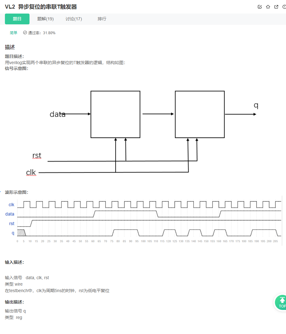
answer
`timescale 1ns/1ns
module Tff_2 (
input wire data, clk, rst,
output reg q
);
//*************code***********//
    reg tmp;
    [email protected](posedge clk or negedge rst)begin
        if (!rst)
            tmp <= 1'd0;
        else if (data)
            tmp <= ~tmp;
        else
            tmp <= tmp;
    end

    [email protected](posedge clk or negedge rst)begin
        if (!rst)
            q <= 1'd0;
        else if (tmp)
            q <= ~q;
        else
            q <= q;
    end
//*************code***********//
endmodule

V2 Asynchronous reset T Series trigger
analysis
T trigger · Baidu Encyclopedia 
- From the picture above, we can see :T The core point of triggers , Come on 1 Flip , Come on 0 keep .
- According to the principle , It is easy to get the above answer . however , Pay attention to the truth table , You will also get a logical expression :
Q* = T ^ Q, So you can simplify the core code :
//*************code***********//
    reg tmp;
    [email protected](posedge clk or negedge rst)begin
        if (!rst)
            tmp <= 1'd0;
        else
            tmp <= data ^ tmp;
    end

    [email protected](posedge clk or negedge rst)begin
        if (!rst)
            q <= 1'd0;
        else
            q <= tmp ^ q;
    end
//*************code***********//
- Pay attention to thinking ,T The core point of triggers , Come on 1 Flip , Come on 0 keep . Can it be understood as , An embodiment of a gated clock ?
replay
Be careful T trigger : Come on 1 Flip , Come on 0 keep .
Pay attention to understanding synchronous reset and asynchronous reset .
Disadvantages of asynchronous reset : Produce burrs ( It is easy to cause metastable state )
Disadvantages of synchronous reset : The circuit realization of synchronous reset , Than asynchronous reset circuit implementation , To waste more circuit resources
About wasting resources , Because of a lot of fpga With asynchronous reset , Therefore, synchronous reset will add one more mux

Then combine the two , Avoid metastable state and make full use of resources , Asynchronous reset and synchronous release can be adopted .
Common asynchronous reset and synchronous release diagram :

The blog here offers answers to a series of points that are often confusing
1. What is the problem with the direct access to the asynchronous reset signal drive reset terminal ?
It is often said that asynchronous reset produces metastable state
2. Two level trigger synchronization , Can metastable states be eliminated ?
You can't , But it can greatly reduce
3. If only one trigger is synchronized , how ?
Can not be . The output of the first stage trigger , There is always the possibility of metastability . Metastable , As a result, the system will not reset and initialize to the known state .
After the first level trigger samples the asynchronous input , The metastable state that allows the output to occur can be as long as one cycle , In this period , The metastable characteristic is weakened . When the second edge of the clock comes , The second stage synchronizer samples , Then the signal is transmitted to the internal logic . The second stage output is stable and synchronized . If the hold time is not enough at the second stage of sampling , The output of the first stage is still in a strong metastable state , This will cause the second stage synchronizer to enter metastable state , But the probability of such failure is relatively small .
4. Reset the synchronizer , The first 2 individual dff Whether there is metastable state ?( This is the most confusing )
Only when DFF Data input port and data output port , There are different values , Just can have recovery timing/removal timing problem .
The first 1 individual dff Data input port and data output port , At the time of asynchronous reset release , yes 1 and 0, So there will be competition and risk , There is a probability of metastable states ;
The first 2 individual dff Data input port and data output port , At the time of asynchronous reset release , yes 0 and 0, So there is no competitive risk , No metastable state is produced .
Because the first 1 individual dff There is a probability of metastable states , To prevent transmission , therefore , Add a few more levels dff, It is beneficial to reduce the probability of metastable propagation .
The answers to 90% of the above questions are transferred from blogs , It's important to note that , Modern digital chip design , The emphasis is on synchronous reset , This is good for STA( Static time series analysis ), Easy to transplant .
RTL Schematic diagram is as follows :
here Q and D The connection I think may be that the logical expression requirements are related to the current state , But tell the truth. , I don't know these two modules RTL The internal structure , No further analysis .
The test code is as follows :

Mainly clk and data Compilation of data
The simulation waveform obtained is as follows :

When data by 1 The moment of , Once the clock samples , The next rising edge of the clock will flip the intermediate output , The intermediate output generates a high level for one cycle every two clock cycles , This leads to a final input flip , Each flip should be done once in two cycles . And it lags behind by one cycle .
When data by 0 When , If the intermediate output is one , The final output continues to flip , If zero , remain unchanged ( The waveform only covers the second result .
VL3 Parity check

answer
`timescale 1ns/1ns
module odd_sel(
input [31:0] bus,
input sel,
output check
);
//*************code***********//

    assign check = sel ? (^bus) : ~(^bus);

//*************code***********//
endmodule

analysis
1、 Parity check , Make... By check bit 1 The number of is just odd or even
Odd check : Original bitstream + Check bit There are an odd number of 1
Even check : Original bitstream + Check bit There are even numbers in total 1
Say something reasonable.,
aboutOdd check, If the original code stream 1 The number of is even , Then the check digit is1, Otherwise, it would be0;
aboutOdd check, If the original code stream 1 The number of is odd , Then the check digit is0, Otherwise, it would be1;
aboutEven check, If the original code stream 1 The number of is even , Then the check digit is0, Otherwise, it would be1;
aboutEven check, If the original code stream 1 The number of is odd , Then the check digit is1, Otherwise, it would be0;
2、 Judge the... In the original code stream 1 Is the number of even or odd
- It's easy to think of XOR here ,
0011_1111_1111_1111The value obtained by bitwise XOR is1, At this time 1 Odd parity bit ; If the parity bit , Take the reverse
3、 Write the pseudo code as follows :
if (sel == 1)// Odd check
	check = ^bus;
else
	check = ~(^bus);
- At this point, it is easy to think of the ternary operator to write the answer :
assign check = sel ? (^bus) : ~(^bus);
replay
- Think carefully here ,
Monocular operatorandReduction operator. It needs a concept , The reduction operator is a unary operator , But a unary operator is not necessarily a reduction operator .

VL4 Shift operation and multiplication

answer
`timescale 1ns/1ns
module multi_sel(
input [7:0]d ,
input clk,
input rst,
output reg input_grant,
output reg [10:0]out
);
//*************code***********//
    reg[1:0] cnt_4;
    [email protected](posedge clk or negedge rst)begin
        if(!rst)
            cnt_4 <= 'd0;
        else if(cnt_4 == 2'b11)
            cnt_4 <= 'd0;
        else cnt_4 <= cnt_4 + 1'b1;
    end

    reg [7:0] d_reg;
    [email protected](posedge clk or negedge rst)begin
        if(!rst)begin
                input_grant <= 'b0;
                out <= 'd0;
        end
        else if(cnt_4 == 'd0)begin
                input_grant <= 'b1;
                d_reg <= d;
                out <= d;
        end
        else if(cnt_4 == 'd1)begin
                input_grant <= 'b0;
                out <= d_reg * 3;
        end

         else if(cnt_4 == 'd2)begin
                input_grant <= 'b0;
                out <= d_reg * 7;
        end

            else if(cnt_4 == 'd3)begin
                input_grant <= 'b0;
                out <= d_reg * 8;
        end
    end
//*************code***********//
endmodule

replay
- In the title, a four beat processing input is clearly given , It is very common to set a counter , Four states can be counted with a two bit counter ,
You don't have to clear the count by yourself. - The above uses... With priority
if -else structure, It can be optimized tocase structure, Xiaobian will not rewrite this part , In the next questioncase structure. - The above signals can be written separately , The optimization effect is as follows :
//*************code***********//
    reg[1:0] cnt_4;
    [email protected](posedge clk or negedge rst)begin
        if(!rst)
            cnt_4 <= 'd0;
        else
            cnt_4 <= cnt_4 + 1'b1;
    end

    reg [7:0] d_reg;
    [email protected](posedge clk or negedge rst)begin
        if(!rst)begin
            input_grant <= 'b0;
            out <= 'd0;
        end
        else if(cnt_4 == 'd0)begin
            d_reg <= d;
            out <= d;
        end
        else if(cnt_4 == 'd1)begin
            out <= d_reg * 3;
        end
         else if(cnt_4 == 'd2)begin
            out <= d_reg * 7;
        end
        else if(cnt_4 == 'd3)begin
            out <= d_reg * 8;
        end
    end

    [email protected](posedge clk or negedge rst)begin
        if(!rst)begin
            input_grant <= 'b0;
        end
        else if(cnt_4 == 'd0)begin
            input_grant <= 'b1;
        end
        else begin
            input_grant <= 'b0;
        end
    end
//*************code***********//
VL5 Bit splitting and operation

answer
`timescale 1ns/1ns

module data_cal(
input clk,
input rst,
input [15:0]d,
input [1:0]sel,

output [4:0]out,
output validout
);
//*************code***********//
    reg validout;
    always @ (posedge clk or negedge rst)begin
        if (!rst)begin
            validout <= 1'b0;
        end
        else if (sel == 2'b0) begin
            validout <= 1'b0;
        end  else begin
            validout <= 1'b1;
        end
    end

    reg [15:0] d_reg;
    always @ (posedge clk or negedge rst)begin
        if (!rst)begin
            d_reg <= 'd0;
        end
        else if (sel == 0)begin
            d_reg <= d;
        end
// else begin
// d_reg <= d_reg;
// end
    end

    reg [4:0]out;
    always @ (posedge clk or negedge rst)begin
        if (!rst)begin
            out <= 'd0;
        end
        else case(sel)
            2'b00:out <= 'd0;
            2'b01:out <= d_reg[3:0] + d_reg[7:4];
            2'b10:out <= d_reg[3:0] + d_reg[11:8];
            2'b11:out <= d_reg[3:0] + d_reg[15:12];
        endcase
    end
//*************code***********//
endmodule

replay
- Pay attention to thinking
d_regThe role of , What role does this signal play , And whether the three lines of commented code can be completely omitted in engineering practice ? case structureHow to deal withif-else structureswap ?
VL6 Multifunctional data processor

answer
`timescale 1ns/1ns
module data_select(
	input clk,
	input rst_n,
	input signed[7:0]a,
	input signed[7:0]b,
	input [1:0]select,
	output reg signed [8:0]c
);

    [email protected](posedge clk or negedge rst_n)begin
        if (!rst_n)
            c <= 'd0;
        else case(select)
            2'b00:c <= a;
            2'b01:c <= b;
            2'b10:c <= a+b;
            2'b11:c <= a-b;
        endcase
    end
endmodule

replay
- Do you think it is completely consistent with the above questions
VL7 Find the difference between two numbers

answer
`timescale 1ns/1ns
module data_minus(
	input clk,
	input rst_n,
	input [7:0]a,
	input [7:0]b,

	output  reg [8:0]c
);
    [email protected](posedge clk or negedge rst_n)
    if (!rst_n)
            c <= 'd0;
    else
        c <= (a > b) ? (a - b) : (b-a);
endmodule
VL8 Use generate…for Statements simplify code

answer
`timescale 1ns/1ns
module gen_for_module(
    input [7:0] data_in,
    output [7:0] data_out
);
    genvar i;
    generate for( i = 0; i < 8; i = i + 1 )
// begin:generate_1
            assign data_out [i] = data_in [7 - i];
// end
    endgenerate

endmodule

replay
- Here are the notes written by others , Look at the answer above , And deliberately put the 2 This message goes against ?
WHY?Surely you can judge for yourself
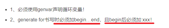

- Also note why the first item needs to be met ? I think it can be combined
Dynamic variablesTo understand !
VL9 Use sub modules to compare the size of three input numbers

answer
`timescale 1ns/1ns
module main_mod(
	input clk,
	input rst_n,
	input [7:0]a,
	input [7:0]b,
	input [7:0]c,

	output [7:0]d
);

    wire [7:0] min1, min2;

   min_mod min1_mod(
       .clk(clk),
       .rst_n(rst_n),
       .a(a),
       .b(b),
       .min(min1)
   );

    min_mod min2_mod(
        .clk(clk),
        .rst_n(rst_n),
        .a(a),
        .b(c),
        .min(min2)
   );

    min_mod min3_mod(
        .clk(clk),
        .rst_n(rst_n),
        .a(min1),
        .b(min2),
        .min(d)
   );
// assign d = min1 > min2 ? min2 : min1;
endmodule


module min_mod(
	input clk,
	input rst_n,
	input [7:0]a,
	input [7:0]b,

    output reg [7:0]min
);
    [email protected](posedge clk or negedge rst_n)
        if(!rst_n)
            min <= 'd0;
        else
            min <= (a > b) ? b : a;

endmodule

replay
- The topic requires the use of sub modules for size comparison
- Pay attention to timing requirements : I wanted to save time , It is written in the following form , I made a mistake .
`timescale 1ns/1ns
module main_mod(
	input clk,
	input rst_n,
	input [7:0]a,
	input [7:0]b,
	input [7:0]c,

	output [7:0]d
);

    wire [7:0] min1, min2;

   min_mod min1_mod(
       .clk(clk),
       .rst_n(rst_n),
       .a(a),
       .b(b),
       .min(min1)
   );

    min_mod min2_mod(
        .clk(clk),
        .rst_n(rst_n),
        .a(a),
        .b(c),
        .min(min2)
   );

// min_mod min3_mod(
// .clk(clk),
// .rst_n(rst_n),
// .a(min1),
// .b(min2),
// .min(d)
// );

    assign d = min1 > min2 ? min2 : min1;

endmodule


module min_mod(
	input clk,
	input rst_n,
	input [7:0]a,
	input [7:0]b,

    output reg [7:0]min
);
    [email protected](posedge clk or negedge rst_n)
        if(!rst_n)
            min <= 'd0;
        else
            min <= (a > b) ? b : a;

endmodule

VL10 Use function to realize data size conversion
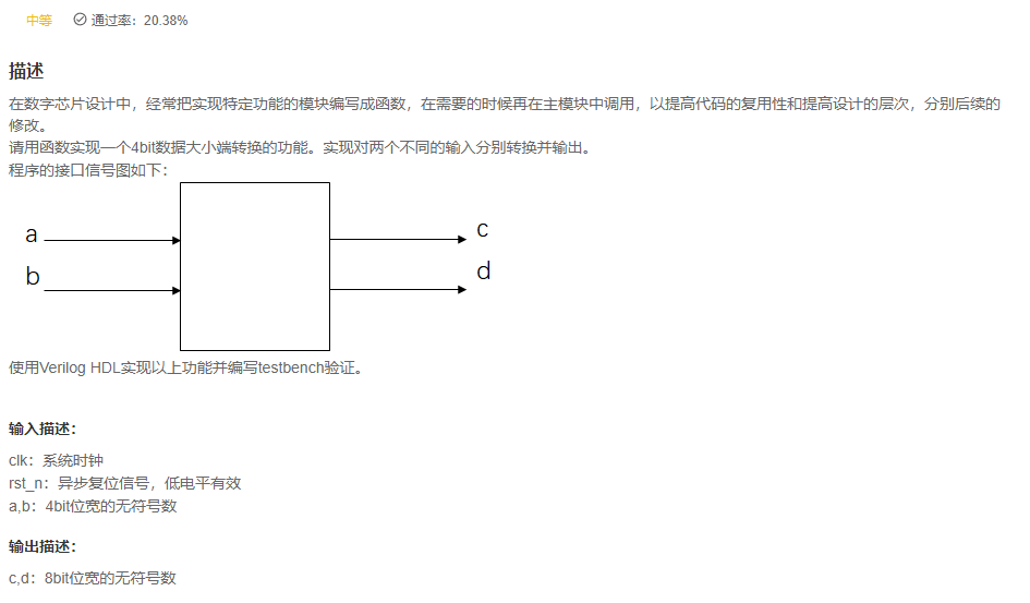
answer
`timescale 1ns/1ns
module function_mod(
    input clk,
    input rst_n,
	input [3:0]a,
	input [3:0]b,

	output [3:0]c,
	output [3:0]d
);

    function [3:0] reverse;
        input [3:0] data_in;
        begin
            reverse[0] = data_in[3];
            reverse[1] = data_in[2];
            reverse[2] = data_in[1];
            reverse[3] = data_in[0];
        end
    endfunction

    assign c = reverse(a);
    assign d = reverse(b);
endmodule

replay
- Don't want to explain more , There is no original port in the title
clkandrst_n, And the title also says ,c and d All are 8bit Of ... - Large and small end , For byte order . This problem can be said to be bit reversal , Besides, , This function is used
Flow operationOne line of code can do , Designers should learn quickly systemverilog.
02. Combinatorial logic
VL11 4 Bit value comparator circuit

answer
`timescale 1ns/1ns

module comparator_4(
	input		[3:0]       A   	,
	input	   [3:0]		B   	,

 	output	 reg		Y2    , //A>B
	output   reg        Y1    , //A=B
    output   reg        Y0      //A<B
);

    [email protected](*)begin
        if (A[3] > B[3])
            {
    Y2,Y1,Y0} = 3'b100;
        else if (A[3] < B[3])
            {
    Y2,Y1,Y0} = 3'b001;
        else if (A[2] > B[2])
            {
    Y2,Y1,Y0} = 3'b100;
        else if (A[2] < B[2])
            {
    Y2,Y1,Y0} = 3'b001;

        else if (A[1] > B[1])
            {
    Y2,Y1,Y0} = 3'b100;
        else if (A[1] < B[1])
            {
    Y2,Y1,Y0} = 3'b001;
        else if (A[0] > B[0])
            {
    Y2,Y1,Y0} = 3'b100;
        else if (A[0] < B[0])
            {
    Y2,Y1,Y0} = 3'b001;
        else
            {
    Y2,Y1,Y0} = 3'b010;
    end

endmodule

replay
- All the above uses
if-elseThis structure , It has a priority relationship , Personally, it seems to be the easiest way to understand . - In the actual project , You don't write a very robust program all at once , The later stage is continuous optimization , Using a variety of advanced algorithms 、 Even add design patterns to optimize .
- The answer to the above question , I define the output port of the interface by
wire typeChange it toreg type, Why? ?( I want to , I just don't want to type ) - Next, we will merge the same output , The code is as follows :
`timescale 1ns/1ns

module comparator_4(
	input		[3:0]       A   	,
	input	   [3:0]		B   	,

 	output	 reg		Y2    , //A>B
	output   reg        Y1    , //A=B
    output   reg        Y0      //A<B
);

    [email protected](*)begin
        if ((A[3] > B[3]) || ((A[3] == B[3]) &&  (A[2] > B[2])) || ((A[3] == B[3]) &&  (A[2] == B[2]) &&  (A[1] > B[1])) || ((A[3] == B[3]) &&  (A[2] == B[2]) &&  (A[1] == B[1]) &&  (A[0] > B[0])))
            {
    Y2,Y1,Y0} = 3'b100;
        else if ((A[3] < B[3]) || ((A[3] == B[3]) &&  (A[2] < B[2])) || ((A[3] == B[3]) &&  (A[2] == B[2]) &&  (A[1] < B[1])) || ((A[3] == B[3]) &&  (A[2] == B[2]) &&  (A[1] == B[1]) &&  (A[0] < B[0])))
            {
    Y2,Y1,Y0} = 3'b001;
        else
            {
    Y2,Y1,Y0} = 3'b010;
    end

endmodule
- Based on the above code , Continue to optimize , The default initial values of variables are 0, We just need to focus on when 1, So continue to optimize , The code is as follows :
`timescale 1ns/1ns

module comparator_4(
	input		[3:0]       A   	,
	input	   [3:0]		B   	,

 	output	 reg		Y2    , //A>B
	output   reg        Y1    , //A=B
    output   reg        Y0      //A<B
);

    [email protected](*)begin
            Y2 = ((A[3] > B[3]) || ((A[3] == B[3]) &&  (A[2] > B[2])) || ((A[3] == B[3]) &&  (A[2] == B[2]) &&  (A[1] > B[1])) || ((A[3] == B[3]) &&  (A[2] == B[2]) &&  (A[1] == B[1]) &&  (A[0] > B[0]))) ? 1'b1 : 1'b0;
            Y0 = ((A[3] < B[3]) || ((A[3] == B[3]) &&  (A[2] < B[2])) || ((A[3] == B[3]) &&  (A[2] == B[2]) &&  (A[1] < B[1])) || ((A[3] == B[3]) &&  (A[2] == B[2]) &&  (A[1] == B[1]) &&  (A[0] < B[0]))) ? 1'b1 : 1'b0;
            Y1 = ((A[3] == B[3]) &&  (A[2] == B[2]) &&  (A[1] == B[1]) &&  (A[0] == B[0]))  ? 1'b1 : 1'b0;
    end

endmodule
- Continue to optimize ,Y1 The logic of can be abbreviated as
Y1 = (A == B) ? 1'b1 : 1'b0;, Even written directly asY1 = A == B;The variables of the three are different 1, therefore except Y1 The variable of can be written as the inverse of the other two variables
`timescale 1ns/1ns

module comparator_4(
	input		[3:0]       A   	,
	input	   [3:0]		B   	,

 	output	 reg		Y2    , //A>B
	output   reg        Y1    , //A=B
    output   reg        Y0      //A<B
);

    [email protected](*)begin
            Y2 = (A[3] > B[3]) || ((A[3] == B[3]) &&  (A[2] > B[2])) || ((A[3] == B[3]) &&  (A[2] == B[2]) &&  (A[1] > B[1])) || ((A[3] == B[3]) &&  (A[2] == B[2]) &&  (A[1] == B[1]) &&  (A[0] > B[0]));
            Y1 = A == B;
            Y0 = ~(Y2 || Y1);
    end

endmodule
- At the moment , Suddenly want to put the output port reg Change the type to the original wire type , Then we need to use assign Statement , Continue to reform , But there was an error , Xiaobian doesn't feel wrong , If you find an error, you can point it out in the comment area .
`timescale 1ns/1ns

module comparator_4(
	input		[3:0]       A   	,
	input	   [3:0]		B   	,

 	output	 wire		Y2    , //A>B
	output   wire       Y1    , //A=B
    output   wire       Y0      //A<B
);

    assign    Y1 = A == B;
    assign    Y2 = (A[3] > B[3]) || ((A[3] == B[3]) &&  (A[2] > B[2])) || ((A[3] == B[3]) &&  (A[2] == B[2]) &&  (A[1] > B[1])) || ((A[3] == B[3]) &&  (A[2] == B[2]) &&  (A[1] == B[1]) &&  (A[0] > B[0]));
    assign    Y0 = ~(Y2 || Y1);

endmodule

VL12 4bit Carry ahead adder circuit

answer
`timescale 1ns/1ns

module lca_4(
	input		[3:0]       A_in  ,
	input	    [3:0]		B_in  ,
    input                   C_1   ,

 	output	 wire			CO    ,
	output   wire [3:0]	    S
);


    wire [3:0] G;
    wire [3:0] P;

    assign G[0] = A_in[0] & B_in[0];
    assign G[1] = A_in[1] & B_in[1];
    assign G[2] = A_in[2] & B_in[2];
    assign G[3] = A_in[3] & B_in[3];

    assign P[0] = A_in[0] ^ B_in[0];
    assign P[1] = A_in[1] ^ B_in[1];
    assign P[2] = A_in[2] ^ B_in[2];
    assign P[3] = A_in[3] ^ B_in[3];

    wire [3:0] C;

    assign S[0] = P[0] ^ C_1;
    assign S[1] = P[1] ^ C[0];
    assign S[2] = P[2] ^ C[1];
    assign S[3] = P[3] ^ C[2];
    assign CO = C[3];

    assign C[0] = G[0] | P[0]&C_1;
    assign C[1] = G[1] | P[1]&C[0];
    assign C[2] = G[2] | P[2]&C[1];
    assign C[3] = G[3] | P[3]&C[2];


endmodule

replay
- Here is an article 3-2 Verilog 4 Bit traveling wave carry adder , You can also learn about
Traveling wave carry (Ripple Carry)AndCarry ahead (Loodahead Carry) - I was very confused at the beginning of my study , This part will not expand nonsense .
VL13 Priority encoder circuit ①

answer
`timescale 1ns/1ns

module encoder_0(
   input      [8:0]         I_n   ,

   output reg [3:0]         Y_n
);
    always @ (*)
      begin
        casex(I_n)
          9'b1_1111_1111 : Y_n = 4'b1111;
          9'b0_xxxx_xxxx : Y_n = 4'b0110;
          9'b1_0xxx_xxxx : Y_n = 4'b0111;
          9'b1_10xx_xxxx : Y_n = 4'b1000;
          9'b1_110x_xxxx : Y_n = 4'b1001;
          9'b1_1110_xxxx : Y_n = 4'b1010;
          9'b1_1111_0xxx : Y_n = 4'b1011;
          9'b1_1111_10xx : Y_n = 4'b1100;
          9'b1_1111_110x : Y_n = 4'b1101;
          9'b1_1111_1110 : Y_n = 4'b1110;
          default : Y_n = 4'b1111;
        endcase
      end
endmodule
replay
- The answer is given in the next question , Ha ha ha
VL14 Use the priority encoder ① Realize the keyboard coding circuit

answer
`timescale 1ns/1ns
module encoder_0(
   input      [8:0]         I_n   ,

   output reg [3:0]         Y_n
);

always @(*)begin
   casex(I_n)
      9'b111111111 : Y_n = 4'b1111;
      9'b0xxxxxxxx : Y_n = 4'b0110;
      9'b10xxxxxxx : Y_n = 4'b0111;
      9'b110xxxxxx : Y_n = 4'b1000;
      9'b1110xxxxx : Y_n = 4'b1001;
      9'b11110xxxx : Y_n = 4'b1010;
      9'b111110xxx : Y_n = 4'b1011;
      9'b1111110xx : Y_n = 4'b1100;
      9'b11111110x : Y_n = 4'b1101;
      9'b111111110 : Y_n = 4'b1110;
      default      : Y_n = 4'b1111;
   endcase
end

endmodule

module key_encoder(
      input      [9:0]         S_n   ,

      output wire[3:0]         L     ,
      output wire              GS
);

    wire   [3:0]  Y_n;
    encoder_0 encoder(
       .I_n   (S_n[9:1]),
       .Y_n   (Y_n)
    );

    assign L = ~Y_n;
// assign GS = ~(S_n[0] & Y_n[0] & Y_n[1] & Y_n[2] & Y_n[3]);
    assign GS = ((Y_n == 4'b1111) && (S_n[0] == 1)) ? 0 : 1;
endmodule

VL15 Priority encoder Ⅰ

answer
`timescale 1ns/1ns

module encoder_83(
   input      [7:0]       I   ,
   input                  EI  ,

   output wire [2:0]      Y   ,
   output wire            GS  ,
   output wire            EO
);
    reg [4:0] temp;
    assign {
    Y[2:0],GS,EO} = temp;
    [email protected](*) begin
        casex({
    EI,I[7:0]})
            9'b0_xxxx_xxxx: temp = 5'b000_00;
            9'b1_0000_0000: temp = 5'b000_01;
            9'b1_1xxx_xxxx: temp = 5'b111_10;
            9'b1_01xx_xxxx: temp = 5'b110_10;
            9'b1_001x_xxxx: temp = 5'b101_10;
            9'b1_0001_xxxx: temp = 5'b100_10;
            9'b1_0000_1xxx: temp = 5'b011_10;
            9'b1_0000_01xx: temp = 5'b010_10;
            9'b1_0000_001x: temp = 5'b001_10;
            9'b1_0000_0001: temp = 5'b000_10;
        endcase
    end
endmodule

replay
- The simplest implementation of this decoder is , You can directly implement the code table once .
- such as , The figures in this part are exactly the same as those in the title
			9'b0_xxxx_xxxx: temp = 5'b000_00;
            9'b1_0000_0000: temp = 5'b000_01;
            9'b1_1xxx_xxxx: temp = 5'b111_10;
            9'b1_01xx_xxxx: temp = 5'b110_10;
            9'b1_001x_xxxx: temp = 5'b101_10;
            9'b1_0001_xxxx: temp = 5'b100_10;
            9'b1_0000_1xxx: temp = 5'b011_10;
            9'b1_0000_01xx: temp = 5'b010_10;
            9'b1_0000_001x: temp = 5'b001_10;
            9'b1_0000_0001: temp = 5'b000_10;
- Of course , There are other implementations , For example, what is given in the following question is
VL16 Use 8 Line -3 Line priority encoder Ⅰ Realization 16 Line -4 Line priority encoder

answer
`timescale 1ns/1ns
module encoder_83(
   input      [7:0]       I   ,
   input                  EI  ,

   output wire [2:0]      Y   ,
   output wire            GS  ,
   output wire            EO
);
assign Y[2] = EI & (I[7] | I[6] | I[5] | I[4]);
assign Y[1] = EI & (I[7] | I[6] | ~I[5]&~I[4]&I[3] | ~I[5]&~I[4]&I[2]);
assign Y[0] = EI & (I[7] | ~I[6]&I[5] | ~I[6]&~I[4]&I[3] | ~I[6]&~I[4]&~I[2]&I[1]);

assign EO = EI&~I[7]&~I[6]&~I[5]&~I[4]&~I[3]&~I[2]&~I[1]&~I[0];

assign GS = EI&(I[7] | I[6] | I[5] | I[4] | I[3] | I[2] | I[1] | I[0]);
//assign GS = EI&(| I);

endmodule

module encoder_164(
   input      [15:0]      A   ,
   input                  EI  ,

   output wire [3:0]      L   ,
   output wire            GS  ,
   output wire            EO
);
    wire [2:0] Y_1,Y_0;
    wire gs_1,gs_0;
    wire EO1;

    encoder_83    encoder_83_U1(
        .I  (A[15:8]),
        .EI (EI),

        .Y  (Y_1),
        .GS (gs_1),
        .EO (EO1)
    );

    encoder_83    encoder_83_U0(
        .I (A[7:0]),
        .EI (EO1),

        .Y  (Y_0),
        .GS (gs_0),
        .EO (EO)
    );
    assign L = {
    gs_1,Y_1[2]|Y_0[2],Y_1[1]|Y_0[1],Y_1[0]|Y_0[0]};
    assign GS = gs_1|gs_0;

endmodule

replay
- Copied , The title is obscure
VL17 use 3-8 The decoder implements a full subtracter

answer
- Do not want to do , Title screenshot , The screenshot will be used as a snapshot to prevent the late update of the question bank
VL18 Realization 3-8 Decoder ①
secondary Passing rate :37.98%
describe
The following table is 74HC138 Decoder menu
① Please use the basic gate circuit to realize the decoder circuit , use Verilog Describe the circuit . The basic gate circuit includes : Not gate 、 Multiple input and gate 、 Multiple input or gate .
Input description :
input E1_n ,
input E2_n ,
input E3 ,
input A0 ,
input A1 ,
input A2
Output description :
output wire Y0_n ,
output wire Y1_n ,
output wire Y2_n ,
output wire Y3_n ,
output wire Y4_n ,
output wire Y5_n ,
output wire Y6_n ,
output wire Y7_n
answer
- Do not want to do , Title screenshot , The screenshot will be used as a snapshot to prevent the late update of the question bank
VL19 Use 3-8 Decoder ① Implement logical functions
- A little
VL20 The data selector implements the logic circuit

answer
`timescale 1ns/1ns

module data_sel(
   input             S0     ,
   input             S1     ,
   input             D0     ,
   input             D1     ,
   input             D2     ,
   input             D3     ,

   output wire        Y
);

assign Y = ~S1 & (~S0&D0 | S0&D1) | S1&(~S0&D2 | S0&D3);

endmodule

module sel_exp(
   input             A     ,
   input             B     ,
   input             C     ,

   output wire       L
);
    data_sel u(
        .S1('b0),
        .S0(C),

        .D1(B),
        .D0(A),
        .Y(L)
    );
endmodule
03. Sequential logic
VL21 Realize sequential circuit according to state transition table

answer
`timescale 1ns/1ns

module seq_circuit(
      input                A   ,
      input                clk ,
      input                rst_n,

      output   wire        Y
);
    reg [1:0] cur_state,next_state;
    reg Y_temp;
    assign Y=Y_temp;

    parameter S0=2'b00;
    parameter S1=2'b01;
    parameter S2=2'b10;
    parameter S3=2'b11;

    [email protected](posedge clk or negedge rst_n)begin
        if(~rst_n)
            cur_state<=S0;
        else
            cur_state<=next_state;
    end

    [email protected](*)begin
        case(cur_state)
            S0:begin
                if(A==0)
                    next_state=S1;
                else
                    next_state=S3;
            end
            S1:begin
                if(A==0)
                    next_state=S2;
                else
                    next_state=S0;
            end
            S2:begin
                if(A==0)
                    next_state=S3;
                else
                    next_state=S1;
            end
            S3:begin
                if(A==0)
                    next_state=S0;
                else
                    next_state=S2;
            end
            default:next_state=S0;
        endcase
    end

    [email protected](*)begin
        if(cur_state==S3)
            Y_temp=1;
        else
            Y_temp=0;
    end

endmodule

replay
Can you understand the following picture

With this watch, draw · The state transition diagram is equivalent to the completion of

Next try to optimize the code .
VL22 Realize sequential circuit according to state transition diagram

answer
`timescale 1ns/1ns

module seq_circuit(
   input                C   ,
   input                clk ,
   input                rst_n,

   output   wire        Y
);

    reg [1:0] cur_state,next_state;
    reg Y_temp;
    assign Y=Y_temp;

    parameter S0=2'b00;
    parameter S1=2'b01;
    parameter S2=2'b10;
    parameter S3=2'b11;

    [email protected](posedge clk or negedge rst_n)begin
        if(~rst_n)
            cur_state<=S0;
        else
            cur_state<=next_state;
    end

    [email protected](*)begin
        case(cur_state)
            S0:begin
                if(C==0)
                    next_state=S0;
                else
                    next_state=S1;
            end
            S1:begin
                if(C==0)
                    next_state=S3;
                else
                    next_state=S1;
            end
            S2:begin
                if(C==0)
                    next_state=S0;
                else
                    next_state=S2;
            end
            S3:begin
                if(C==0)
                    next_state=S3;
                else
                    next_state=S2;
            end
            default:next_state=S0;
        endcase
    end

    [email protected](*)begin
        if(cur_state==S3 || (cur_state==S2 && C == 1))
            Y_temp=1;
        else
            Y_temp=0;
    end


endmodule

replay
- Directly modify the code of the previous question
VL23 ROM Simple implementation of

answer
`timescale 1ns/1ns
module rom(
	input clk,
	input rst_n,
	input [7:0]addr,

	output [3:0]data
);

    reg [3:0] romreg[7:0];

    always @ (posedge clk or negedge rst_n)
    begin
        if( ~rst_n ) begin
            romreg[0] <= 4'd0;
            romreg[1] <= 4'd2;
            romreg[2] <= 4'd4;
            romreg[3] <= 4'd6;
            romreg[4] <= 4'd8;
            romreg[5] <= 4'd10;
            romreg[6] <= 4'd12;
            romreg[7] <= 4'd14;
        end
// else begin
// romreg[0] <= 4'd0;
// romreg[1] <= 4'd2;
// romreg[2] <= 4'd4;
// romreg[3] <= 4'd6;
// romreg[4] <= 4'd8;
// romreg[5] <= 4'd10;
// romreg[6] <= 4'd12;
// romreg[7] <= 4'd14;
// end
    end

    assign data = romreg[addr];

endmodule

replay
- Actually, this read-only register , It will not change after initialization , So it just needs to be in
assignmentThe initial value can be assigned when the , In the actual project, we usually passRead Men The configuration fileTo initialize the . - Regular initialization , It will not be assigned by one , Find the rules , It can be developed quickly . The optimization code is as follows :
`timescale 1ns/1ns
module rom(
	input clk,
	input rst_n,
	input [7:0]addr,

	output [3:0]data
);

    reg [3:0] romreg[7:0];
    integer i;
    always @ (posedge clk or negedge rst_n)
        if( ~rst_n ) begin
            for(i = 0; i < 8; i = i+1) begin : rom_i
                romreg[i] <= 2*i;
            end
        end

    assign data = romreg[addr];

endmodule
VL24 Edge detection
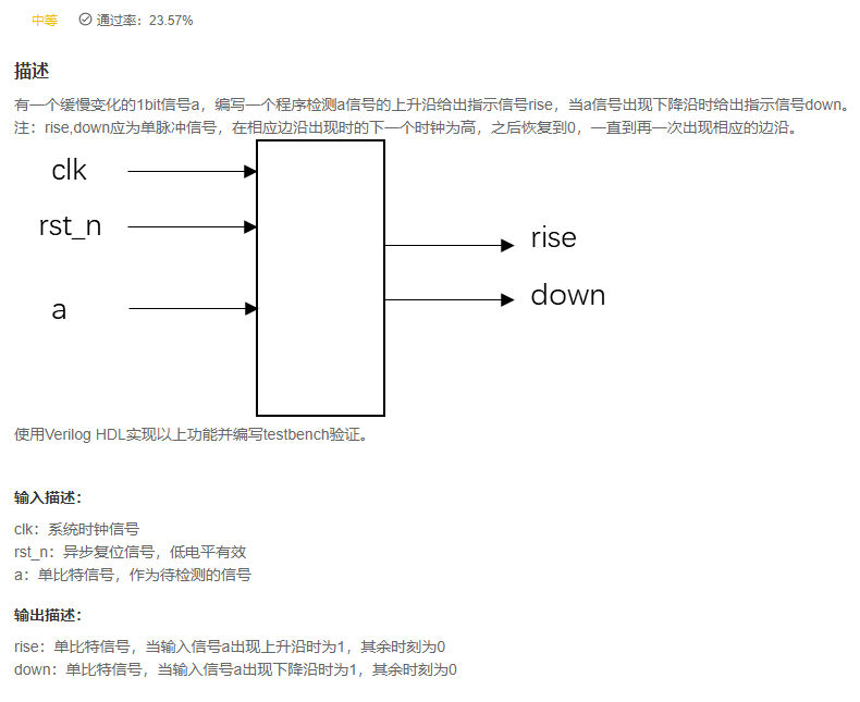
answer
`timescale 1ns/1ns
module edge_detect(
	input clk,
	input rst_n,
	input a,

	output reg rise,
	output reg down
);

    reg a_reg;

    [email protected](posedge clk or negedge rst_n)
        if(!rst_n)begin
            a_reg <= 1'b0;
            rise <= 1'b0;
            down <= 1'b0;
        end
        else begin
            a_reg <= a;
            if(a & ~a_reg)
                rise <= 1'b1;
            else
                rise <= 1'b0;
            if(~a & a_reg)
                down <= 1'b1;
            else
                down <= 1'b0;
        end

endmodule

replay
- Pay attention to the examination , The title clearly says ,
The next edge of the clock will be raised, signify , You can no longer use two-level registers for two beats .
Part II Verilog Advanced challenges
Part III Verilog Enterprise truth
Postscript
Recommend related articles
边栏推荐
- Laravel document sorting 3. CSRF protection
- js中的concat()
- Finereport (sail soft) handling the problem that the histogram data label is blocked
- PostgreSQL数据库WAL——RM_HEAP_ID日志记录动作
- 无法安装redis接口
- Intel 13th generation core showed its true colors for the first time: 68mb cache improved significantly
- PHP encapsulates curl to send get and post request methods, and uses
- 记录小知识点
- js的call()和apply()
- EasyRecovery15非常好用的电脑数据恢复软件
猜你喜欢

Record small knowledge points

PHP extracts and analyzes table contents, and collects bidding information

OBS Browser+浏览器的基本使用

unity Quad剔除背面并剔除透明部分的shader

【esp32学习之路6——flash加密】

Can Navicat directly operate the Android database SQLite

Failed to install redis interface

GBASE 8s 总体架构
![Leetcode points to the leetcode road of offering II 091 house painting [dynamic planning] heroding](/img/ad/69fce7cf064479a0ddd477fb935de2.png)
Leetcode points to the leetcode road of offering II 091 house painting [dynamic planning] heroding

CTF_ Web: basic 12 questions WP of attack and defense world novice zone
随机推荐
Gbase 8s stored procedure flow control
Unit test coverage
领导:谁再用 Redis 过期监听实现关闭订单,立马滚蛋!
js中的concat()
Xiaobai learns MySQL - Statistical 'opportunism'
CTF_ Web: Advanced questions of attack and defense world expert zone WP (9-14)
CTF_ Web: basic 12 questions WP of attack and defense world novice zone
Use of deferred environment variable in gbase 8s
Multithreading structure of gbase 8s
PHP extracts and analyzes table contents, and collects bidding information
515. 在每个树行中找最大值 / 剑指 Offer II 095. 最长公共子序列
Doubts about judging the tinyint field type of MySQL
GBASE 8s 总体架构
What is persistence? What are RDB and AOF in redis persistence?
Structure syntaxique des procédures stockées gbase 8S
GBASE 8s 索引R树
GBASE 8s的隔离级别介绍
Value transfer between parent and child components of wechat applet
Gbase 8s parallel operation problem scenario description
cnpm : 无法加载文件 C:\Users\Administrator\AppData\Roaming\npm\cnpm.ps1,因为在此系统上禁止运行脚本。