当前位置:网站首页>Precautions for running high-frequency and high-speed signal lines near PCB board - basic principles for high-frequency and high-speed signal design
Precautions for running high-frequency and high-speed signal lines near PCB board - basic principles for high-frequency and high-speed signal design
2022-06-23 04:47:00 【Boundless also initial heart】
We often read in textbooks or in the original factory PCB Design Guide See some design principles for high-frequency and high-speed signals , It includes PCB Do not use high-speed signal lines at the edge of the circuit board , For on-board PCB Antenna design , It is also recommended that the antenna should be placed as close to the board edge as possible . fuck , What is the scientific truth ? Old here wu Combined with some of my shallow knowledge , Let's talk about the high-frequency and high-speed signal lines in PCB What happens to the edge of the board , The following represents the old wu My personal point of view , There is no guarantee of correctness , Please identify by yourself ,O(∩_∩)O~
We already know in junior high school , The right hand rule tells us that , The current in the wire travels in the direction of the thumb , Then a corresponding magnetic field will be generated on the conductor , The direction of the magnetic field is the same as that of the fist clenched by the fingers of the right hand , The electric charge in the conductor will generate an electric field , Electric and magnetic fields are good friends , Collectively referred to as electromagnetic fields . 
Ampere right hand screw rule
According to Maxwell's electromagnetic field theory , A changing electric field produces a changing magnetic field in its surrounding space , And the changing magnetic field will produce the changing electric field . such , There is an interdependence between the changing electric field and the changing magnetic field , Mutual excitation , Alternately produce , And spread out in space from near to far at a certain speed , This is electromagnetic radiation . This has two diametrically opposite effects : The good , be-all RF signal communication 、 Wireless Internet 、 Inductive applications benefit from the benefits of electromagnetic radiation ; The harmful aspect is , Electromagnetic radiation leads to crosstalk and electromagnetic compatibility problems . 
When the frequency of electromagnetic wave is low , It is mainly through a tangible conductor that it can be transmitted ; As the frequency increases , Electromagnetic waves will spill out of the conductor , It can transfer energy without medium , This is a kind of radiation . In low-frequency electrical oscillations , The mutual change between magnetoelectricity is relatively slow , Almost all of its energy is returned to the original circuit without energy radiation . However , In high frequency electrical oscillations , Magnetoelectric interconversion is very fast , It is impossible for the energy to return to the original oscillation circuit , So electricity 、 With the periodic change of electric field and magnetic field, magnetic energy propagates to space in the form of electromagnetic wave .
According to the above theory , Each section of wire flowing through high-frequency current will have electromagnetic radiation , The radiation intensity is proportional to the frequency .PCB Some wires on the are used for signal transmission , Such as DDR Clock signal ,LVDS Differential signal transmission line, etc , You don't want too much electromagnetic radiation to lose energy and cause interference to other circuits in the system ; Some wires are used as antennas , Such as PCB The antenna , I hope to convert energy into electromagnetic waves and send them out as much as possible .
about PCB For high-speed signal transmission lines on ( Such as :DDR Clock signal ,HDMI LVDS High speed differential transmission line ), We always want to minimize the radiation generated during signal transmission , Some experts have summarized some design principles to reduce the electromagnetic radiation generated by signal transmission lines , To reduce the of the signal transmission line EMI, Make the distance between the signal transmission line and the reference plane constituting the signal return path as close as possible , If the width of the transmission line W Distance from reference plane H The ratio of is less than 1:3, The external radiation intensity of the microstrip transmission line can be significantly reduced .
For microstrip transmission lines , Using a wide and complete reference plane can also reduce the external radiation intensity of the electric field , The reference plane corresponding to the microstrip transmission line must be at least the 3 Times the width , The wider the reference plane, the better .


If the reference plane is not wide enough relative to the micro single transmission line , The coupling between the electric field and the reference plane is small , The radiation from the electric field increases significantly .
So , If we want to reduce the electromagnetic radiation of high signal transmission microstrip line , The reference plane corresponding to the microstrip transmission line should be as large as possible , If the high-speed microstrip transmission line is close to PCB If the board edge is parallel to the line , Relatively speaking , The reference plane is less coupled to the high-speed signal line , Naturally, it will cause a significant increase in the external radiation of the electric field .

Empathy , High speed IC, The crystal oscillator shall also be placed away from the board edge as far as possible , High speed IC It also needs a complete and wide reference plane for electromagnetic coupling , To reduce EMI.
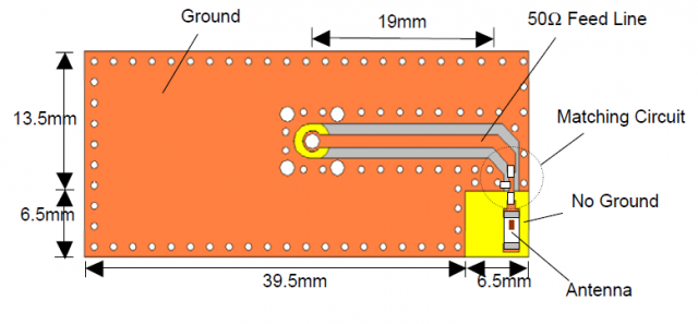
For onboard antennas , We hope to radiate electromagnetic waves into space as much as possible , Therefore, the design principle of onboard antenna is opposite to that of high-speed transmission line , The onboard antenna needs to be placed at the edge of the board , Moreover, the position of the antenna area shall be free of copper foil plane , Yes , All layers need to be set with a copper foil prohibition zone . And the antenna should be connected with PCB The ground level of .
summary :
The same theory , There are different design principles for different applications , The knowledge of electronic design is really broad and profound , It's not something that happens overnight . It's just like that old saying , Three generations of poor farmers , Electrons destroy life … Be careful, be careful ! The old wu I advise you to be cautious when entering the industry O(∩_∩)O~
Reprinted from Wu Chuanbin's blog http://www.mr-wu.cn/
边栏推荐
猜你喜欢

CVE-2019-14287(sudo提权)

LabVIEW displays both hexadecimal and normal characters in the same table
重装Cadence16.3,失败与成功

在Pycharm中对字典的键值作更新时提示“This dictionary creation could be rewritten as a dictionary literal ”的解决方法

Halcon知识:binocular_disparity 知识

How does flutter achieve different zoom animation effects

How to use shell script to monitor file changes

语料库数据处理个案实例(词性赋码、词性还原)

Monitoring artifact ZABBIX, from deployment to application, goes deep layer by layer

Abnova 荧光染料 555-C3 马来酰亚胺方案
随机推荐
20000 words + 20 pictures | details of nine data types and application scenarios of redis
zk 有一个节点报 It is probably not running且日志无明显报错
Permission Operation in dynamics 365 plug-in
第二次作业笔记
积分商城的三种运营方向
const理解之二
离线数仓建模中常见的概念-术语
自动化测试常见的面试题
[pytoch] calculate the derivative of sin (x) by automatic differentiation
Laravel 通过服务提供者来自定义分页样式
C语言刷题随记 —— 自由落体的球
golang使用mongo-driver操作——增(基础)
How does flutter achieve different zoom animation effects
开关磁阻电机悬浮驱动IR2128小结
Openjudge noi 1.13 51: ancient password
notepad++ 查找替换之分组替换保留
解决使用Exception抛出后,@Transactional不生效
磁阻 磁饱和
Please use the NLTK Downloader to obtain the resource
力扣今日题513. 找树左下角的值