当前位置:网站首页>PCB design skills of EMC
PCB design skills of EMC
2022-07-28 07:39:00 【Risehuxyc】
Electromagnetic compatibility (EMC) And associated electromagnetic interference (EMI) System design engineers have always been required to keep their eyes open , Nowadays, circuit board design and component packaging are shrinking 、OEM When a higher speed system is required , These two major problems are particularly PCB Layout and design engineers have a headache .
EMC And the generation of electromagnetic energy 、 Communication and reception are closely related ,PCB Don't want to appear in the design EMC. Electromagnetic energy comes from multiple sources , They mix together , Therefore, special care must be taken , Ensure different circuits 、 Routing 、 Via and PCB When materials work together , Various signals are compatible and will not interfere with each other .
On the other hand ,EMI By EMC Or a destructive effect of unwanted electromagnetic energy . In this electromagnetic environment ,PCB Designers must ensure that the generation of electromagnetic energy is reduced , Minimize interference .
To avoid the PCB Electromagnetic problems in the design 7 Tips
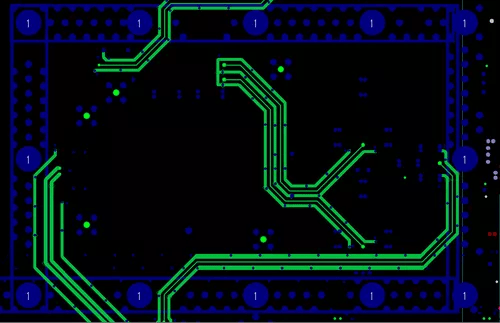
skill 1: take PCB Grounding
Reduce EMI One of the important ways is to design PCB Ground plane . The first step is to make PCB The grounding area within the total area of the circuit board shall be as large as possible , This will reduce emissions 、 Crosstalk and noise . Special care must be taken when connecting each component to the ground point or ground plane , If you don't do that , The neutralization effect of reliable ground formation cannot be fully utilized .
A particularly complex PCB The design has several stable voltages . Ideally , Each reference voltage has its own corresponding ground plane . however , If there are too many ground layers, it will increase PCB The cost of manufacturing , Make the price too high . The compromise is to use ground planes at three to five different locations , Each grounding layer can contain multiple grounding parts . This not only controls the manufacturing cost of the circuit board , It also reduces EMI and EMC.
If you want to make EMC Minimum , Low impedance grounding system is very important . In the multilayer PCB in , It is better to have a reliable ground plane , Instead of a copper counterweight (copper thieving) Or scattered ground plane , Because it has low impedance , It can provide current path , It is the best reverse signal source .
The length of time the signal returns to the ground is also very important . The time for the signal to and from the signal source must be equal , Otherwise, the phenomenon similar to antenna will occur , Make the radiant energy become EMI Part of . Again , towards / The route of transmitting current from the signal source should be as short as possible , If the length of the source path and the return path are not equal , Will produce grounding rebound , It also produces EMI.
If the time of the signal entering and leaving the signal source is not synchronized , It will produce a phenomenon similar to antenna , Thus radiating energy , cause EMI
skill 2: distinguish EMI
because EMI Different , A good one EMC The design rule is to separate analog circuits from digital circuits . Analog circuits have higher amperage or current , Keep away from high-speed wiring or switching signals . If possible , They should be protected with grounding signals . In the multilayer PCB On , The wiring of analog wiring should be on a ground plane , The switch wiring or high-speed wiring should be on another ground plane . therefore , Signals with different characteristics are separated .
Sometimes a low-pass filter can be used to eliminate the high-frequency noise coupled with the surrounding wiring . Filter can suppress noise , Return stable current . It is important to separate the ground plane of analog signal and digital signal . Because analog circuit and digital circuit have their own unique characteristics , It's important to separate them . Digital signal should have digital grounding , The analog signal should terminate at the analog ground .
In digital circuit design , experienced PCB Layout and design engineers will pay special attention to high-speed signals and clocks . At high speed , Signals and clocks should be as short as possible and adjacent to the ground plane , Because as mentioned before , The ground plane can make crosstalk 、 Noise and radiation are kept within controllable range .
Digital signals should also be away from the power plane . If it's close , Will produce noise or induction , Thus weakening the signal .
skill 3: Crosstalk and routing are the key points
Wiring is particularly important to ensure the normal flow of current . If the current comes from an oscillator or other similar device , Then separate the current from the ground plane , Or don't let the current run in parallel with another line , Especially important . Two parallel high-speed signals will be generated EMC and EMI, Especially crosstalk . The resistance path must be minimized , The return current path is also as short as possible . The length of the return path route should be the same as that of the transmission route .
about EMI, One is called “ Violation of routing ”, The other is “ Victim routing ”. Inductive and capacitive coupling will be affected by the existence of electromagnetic fields “ Victimization ” Routing , Thus in “ Victim routing ” Generate forward and reverse currents . In this case , Ripple will occur in a stable environment where the transmission length and reception length of the signal are almost the same .
In a good balance 、 In a stable environment , The induced currents should cancel each other , Thus eliminating crosstalk . however , We live in an imperfect world , Such a thing will not happen . therefore , Our goal is to keep the crosstalk of all lines to a minimum . If the width between parallel routes is twice the route width , Then the influence of crosstalk can be minimized . for example , If the wiring width is 5 Mils , Then the minimum distance between two parallel routes should be 10 Mils or more .
With the continuous emergence of new materials and new components ,PCB Designers must also continue to deal with electromagnetic compatibility and interference .
skill 4: Decoupling capacitor
Decoupling capacitance can reduce the adverse effects of crosstalk , They should be located between the power and ground pins of the equipment , This ensures a low AC impedance , Reduce noise and crosstalk . In order to achieve low impedance in a wide frequency range , Multiple decoupling capacitors should be used .
An important principle for placing decoupling capacitors is , The capacitor with the smallest capacitance value should be as close to the equipment as possible , To reduce the inductive effect on the wiring . This particular capacitor should be as close to the power pin or power line of the device as possible , And connect the bonding pad of the capacitor directly to the via or ground plane . If the route is long , Please use multiple vias , Minimize grounding impedance .
skill 5: avoid 90° horn
To reduce EMI, Wiring should be avoided 、 Through holes and other components form 90° horn , Because right angles produce radiation . The capacitance will increase at this corner , The characteristic impedance will also change , Cause reflection , Then cause EMI. To avoid 90° horn , The routing should be at least two 45° Corner wiring to the corner .
skill 6: Be careful when using vias
In almost all PCB Layout , Vias must be used to provide conductive connections between different layers .PCB Layout engineers need to be very careful , Because the via hole will produce inductance and capacitance . In some cases , They also produce reflections , Because when making vias in wiring , The characteristic impedance will change .
Also remember , Through holes will increase the length of wiring , It needs to be matched . If it is differential routing , Through holes should be avoided as far as possible . If you can't avoid , Then vias should be used in both routes , To compensate for delays in the signal and return path .
skill 7: Cables and physical shielding
Cables carrying digital circuits and analog currents will generate parasitic capacitance and inductance , Cause a lot of EMC Related issues . If twisted pair cable is used , Will maintain a low coupling level , Eliminate the generated magnetic field . For high frequency signals , Shielded cables must be used , Its front and back are grounded , eliminate EMI interfere .
Physical shielding is to wrap the whole or part of the system with a metal package , prevent EMI Get into PCB circuit . This shield is like a closed grounded conductive container , It can reduce the size of antenna loop and absorb EMI.
边栏推荐
- Heroku operation summary
- 登录模式:单一服务器模式、单点登录、token模式
- EMC rectification ideas
- ArcGIS JS customizes the accessor and uses the watchutils related method to view the attribute
- Collection | combined with my personal experience, I have summarized these seven EMC related knowledge
- 每日一题——分割等和子集
- The cornerstone of EMC - complete knowledge of electromagnetic compatibility filtering!
- Eventbus of guava
- Which of class A and class B is more stringent in EMC?
- 4.1.4 why set the member variable to private
猜你喜欢

Safflower STL
![[solution] visual full link log tracking - log tracking system](/img/0c/f93c7d31e01257c5dee7d292ac7d84.jpg)
[solution] visual full link log tracking - log tracking system

数据化管理洞悉零售及电子商务运营——数据化管理介绍

Matplotlib绘图笔记基础直线、折线、曲线

CAS vs Database optimistic lock

Big talk persistence and redolog

Essential performance optimization topics in the interview~

Clion debugging redis6 source code

Not used for the longest time recently

【jvm优化超详细】常见的JVM调优场景
随机推荐
flow_ x+flow_ y---RGB
两个星期学会软件测试?我震惊了!
【jvm优化】线上JVM调优实践
一口气学完4种 Redis 集群方案,真是各有千秋
DNA-Ag2SQDs脱氧核糖核酸DNA修饰硫化银Ag2S量子点的合成方法
调整数组顺序使奇数位于偶数前面——每日两题
Safflower STL
指针进阶练习
xmpp 服务研究(二) prosody 创建账户
node(一)
EMC整改思路
2022年湖南工学院ACM集训第五次周测AD题题解
5G 商用第三年:无人驾驶的“上山”与“下海”
MySQL basic knowledge learning (II)
ArcGIS JS customizes the accessor and uses the watchutils related method to view the attribute
Summary of project experience
EMC中的基石-电磁兼容滤波知识大全!
C语言详解系列——数组详解,一维数组、二维数组
【干货】32个EMC标准电路分享!
和为s的两个数字——每日两题