当前位置:网站首页>FPGA flash reading and writing based on SPI
FPGA flash reading and writing based on SPI
2022-07-23 19:08:00 【qq_ forty-four million nine hundred and eighty-five thousand si】
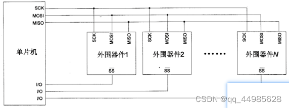
One 、SPI
SPI The principle of communication is very simple , It works in a master-slave way , This mode usually has a master device and one or more slave devices , You need at least 4 Root line , in fact 3 Roots can also ( One way transmission ). It's all based on SPI It's shared by all kinds of devices , They are MISO( Main equipment data input )、MOSI( Main device data output )、SCLK( The clock )、CS( Chip selection ).
(1)MISO– Master Input Slave Output, Main equipment data input , Output data from device ;
(2)MOSI– Master Output Slave Input, Main device data output , From device data input ;
(3)SCLK – Serial Clock, Clock signal , Generated by the main equipment ;
(4)CS – Chip Select, Slave enable signal , Controlled by the main equipment .
Two 、 see spi–flash Find the key
1. describe 
16Mbit Storage space
Single sector erase or whole block erase
use spi Deal with the flash Reading and writing
2.flash Interface signal 

C It's a serial clock
D Is the data
S It's a selection signal
3.SPI Mode selection
flash Only support mode0 and mode3 Two modes 
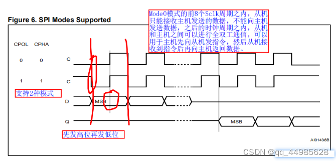
CPOL Clock phase
The polarity of the clock (CPOL) Used to determine when the bus is idle , Synchronous clock (SCK) Whether the potential on the signal line is high or low . At that time, the polarity of the clock was 0 when (CPOL=0),SCK The signal line is low when idle ; At that time, the polarity of the clock was 1 when (CPOL=1),SCK The signal line is high when idle ;
CPHA Clock polarity
At that time, the phase of the clock is 1 when (CPHA=1), stay SCK The second jump edge of the signal line is sampled ; Whether the jump edge here is a rising edge or a falling edge ? Depending on the polarity of the clock . At that time, the polarity of the clock was 0 when , Take the falling edge ; At that time, the polarity of the clock was 1 when , Take the rising edge
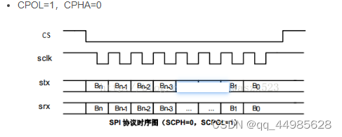
CPOL=0,CPHA=0


4. High byte MSB
MSB First , High byte first
5. Instructions 

6. Write enable sequence 
7. read ID sequential 
8. Read register timing ( I didn't use )
Judge WIP BIT Is it 0 To move on ( I don't use... In my code )
9. Read data timing 
10. Page programming 
11. Sector erase 
12. Important time 
3、 ... and 、 State machine design
1.spi Interface state machine 
2.flash Read state machine 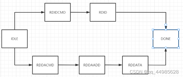
3.flash Write state machine 
Four 、 Code section
1.spi_interface.v
module spi_interface(
    input           clk,
    input           rst_n,
    //  Interface with host
    input   [7:0]   din,
    input           req,
    output  [7:0]   dout,
    output          done,
    //  Interface and flash
    input           miso,//  The master sample is sent from the slave
    output          mosi,//  The master sends the slave
    output          sclk,//  The serial clock
    output          cs_n //  Piece of optional signal
);

parameter   CPHA = 1,//  Idle state high level
            CPOL = 1;//  The falling edge sends , Rising edge sampling

// 16 Frequency division or 8 Frequency division or 4 frequency division   You can't 2 frequency division
parameter   SCLK = 16,
            SCLK_BEFORE = SCLK/4,
            SCLK_AFTER  = SCLK*3/4;

//  State machine
localparam  IDLE  = 4'b0001,
            WAIT  = 4'b0010,
            DATA  = 4'b0100,
            DONE  = 4'b1000;

reg     [3:0]       state_c;
reg     [3:0]       state_n;

wire                idle2wait;
wire                wait2data;
wire                data2done;
wire                done2idle;

// bit Counter
reg     [2:0]       cnt_bit;
wire                add_cnt_bit;
wire                end_cnt_bit;

//  Frequency division serial clock counter
reg     [4:0]       cnt_sclk;
wire                add_cnt_sclk;
wire                end_cnt_sclk;

//  Register the data to be sent
reg                 spi_sclk;
reg     [7:0]       rx_data;
reg     [7:0]       tx_data;
reg                 spi_cn_n;
always @(posedge clk or negedge rst_n)begin
    if(!rst_n)begin
        state_c <= IDLE;
    end
    else begin
        state_c <= state_n;
    end
end

always @(*)begin
    case (state_c)
        IDLE      :begin
                    if(idle2wait)begin
                        state_n = WAIT;
                    end
                    else begin
                        state_n = state_c;
                    end
                   end
        WAIT      :begin
                    if(wait2data)begin
                        state_n = DATA;
                    end
                    else begin
                        state_n = state_c;
                    end
                   end
        DATA      :begin
                    if(data2done)begin
                        state_n = DONE;
                    end
                    else begin
                        state_n = state_c;
                    end
                   end
        DONE      :begin
                    if(done2idle)begin
                        state_n = IDLE;
                    end
                    else begin
                        state_n = state_c;
                    end
                   end
        default: state_n = IDLE;
    endcase
end

assign idle2wait = state_c == IDLE && (req);
assign wait2data = state_c == WAIT && (1'b1);
assign data2done = state_c == DATA && (end_cnt_bit);
assign done2idle = state_c == DONE && (1'b1);

// bit Counter
always @(posedge clk or negedge rst_n)begin
   if(!rst_n)begin
        cnt_bit <= 0;
    end
    else if(add_cnt_bit)begin
            if(end_cnt_bit)begin
                cnt_bit <= 0;
            end
            else begin
                cnt_bit <= cnt_bit + 1;
            end
    end
   else  begin
       cnt_bit <= cnt_bit;
    end
end

assign add_cnt_bit = end_cnt_sclk;
assign end_cnt_bit = add_cnt_bit && cnt_bit == 8 - 1;

// sclk Counter
always @(posedge clk or negedge rst_n)begin
   if(!rst_n)begin
        cnt_sclk <= 0;
    end
    else if(add_cnt_sclk)begin
            if(end_cnt_sclk)begin
                cnt_sclk <= 0;
            end
            else begin
                cnt_sclk <= cnt_sclk + 1;
            end
    end
   else  begin
       cnt_sclk <= cnt_sclk;
    end
end

assign add_cnt_sclk = (state_c == DATA);
assign end_cnt_sclk = add_cnt_sclk && cnt_sclk == SCLK - 1;

// 16 Frequency division serial clock  CPHA=1,CPOL=1
always @(posedge clk or negedge rst_n)begin
    if(!rst_n)begin
        if(CPHA == 0)begin
            spi_sclk <= 1'b0;
        end
        else if(CPHA == 1)begin
            spi_sclk <= 1'b1;
        end
    end
    else if(add_cnt_sclk && cnt_sclk == SCLK_BEFORE - 1)begin
        if(CPHA == 0)begin
            spi_sclk <= 1'b1;
        end
        else if(CPHA == 1)begin
            spi_sclk <= 1'b0;
        end
    end
    else if(add_cnt_sclk && cnt_sclk == SCLK_AFTER - 1)begin
        if(CPHA == 0)begin
            spi_sclk <= 1'b0;
        end
        else if(CPHA == 1)begin
            spi_sclk <= 1'b1;
        end
    end
end

//  Data sent mosi  High position MSB First  CPHA=1,CPOL=1
always @(posedge clk or negedge rst_n)begin
    if(!rst_n)begin
        tx_data <= 0;
    end
    else if(CPOL == 0)begin
        if(add_cnt_sclk && cnt_sclk == SCLK_AFTER - 1)begin
            tx_data <= din;
        end
    end
    else if(CPOL == 1)begin
        if(add_cnt_sclk && cnt_sclk == SCLK_BEFORE - 1)begin
            tx_data <= din;
        end
    end
end

//  Data received miso  High position MSB First  CPHA=1,CPOL=1
always @(posedge clk or negedge rst_n)begin
    if(!rst_n)begin
        rx_data <= 0;
    end
    else if(CPOL == 0)begin
        if(add_cnt_sclk && cnt_sclk == SCLK_BEFORE - 1)begin
            rx_data[7-cnt_bit] <= miso;
        end
    end
    else if(CPOL == 1)begin
        if(add_cnt_sclk && cnt_sclk == SCLK_AFTER - 1)begin
            rx_data[7-cnt_bit] <= miso;
        end
    end
end

assign mosi = tx_data[7-cnt_bit];
assign sclk = spi_sclk;
assign cs_n = ~req;
assign dout = rx_data;
assign done = (state_c == DONE);

endmodule
2.spi_read_ctrl.v
module spi_read_ctrl(
    input               clk,
    input               rst_n,
    input       [2:0]   key_out,
    input       [7:0]   din,
    input               done,
    output reg          req,
    output      [7:0]   dout,
    output reg  [23:0]  seg_data
);

localparam  RDID_CMD = 8'h9F,//  read ID Instructions
            RDDA_CMD = 8'h03,//  Read data command
            RDDA_ADD = 24'h0;//  Read data address

localparam  IDLE    = 7'b000_0001,
            RDIDCMD = 7'b000_0010,
            RDID    = 7'b000_0100,
            RDDACMD = 7'b000_1000,
            RDDAADD = 7'b001_0000,
            RDDATA  = 7'b010_0000,
            DONE    = 7'b100_0000;

reg     [6:0]       state_c;
reg     [6:0]       state_n;

wire                idle2rdidcmd   ;
wire                idle2rddacmd   ;
wire                rdidcmd2rdid   ;
wire                rdid2done      ;
wire                rddacmd2rddaadd;
wire                rddaadd2rddata ;
wire                rddata2done    ;
wire                done2idle      ;

//  Byte counter
reg     [2:0]       cnt_byte;
wire                add_cnt_byte;
wire                end_cnt_byte;

//  read id And read data requests
reg                 rdid_req;
reg                 rdda_req;

reg     [7:0]       tx_data;
//  State machine
always @(posedge clk or negedge rst_n)begin
    if(!rst_n)begin
        state_c <= IDLE;
    end
    else begin
        state_c <= state_n;
    end
end

always @(*)begin
    case (state_c)
        IDLE      :begin
                    if(idle2rdidcmd)begin
                        state_n = RDIDCMD;
                    end
                    else if(idle2rddacmd)begin
                        state_n = RDDACMD;
                    end
                    else begin
                        state_n = state_c;
                    end
                   end
        RDIDCMD      :begin
                    if(rdidcmd2rdid)begin
                        state_n = RDID;
                    end
                    else begin
                        state_n = state_c;
                    end
                   end
        RDID      :begin
                    if(rdid2done)begin
                        state_n = DONE;
                    end
                    else begin
                        state_n = state_c;
                    end
                   end
        RDDACMD      :begin
                    if(rddacmd2rddaadd)begin
                        state_n = RDDAADD;
                    end
                    else begin
                        state_n = state_c;
                    end
                   end
        RDDAADD      :begin
                    if(rddaadd2rddata)begin
                        state_n = RDDATA;
                    end
                    else begin
                        state_n = state_c;
                    end
                   end
        RDDATA      :begin
                    if(rddata2done)begin
                        state_n = DONE;
                    end
                    else begin
                        state_n = state_c;
                    end
                   end
        DONE      :begin
                    if(done2idle)begin
                        state_n = IDLE;
                    end
                    else begin
                        state_n = state_c;
                    end
                   end
        default: state_n = IDLE;
    endcase
end

assign idle2rdidcmd     = state_c == IDLE       && (rdid_req);
assign idle2rddacmd     = state_c == IDLE       && (rdda_req);
assign rdidcmd2rdid     = state_c == RDIDCMD    && (end_cnt_byte);
assign rdid2done        = state_c == RDID       && (end_cnt_byte);
assign rddacmd2rddaadd  = state_c == RDDACMD    && (end_cnt_byte);
assign rddaadd2rddata   = state_c == RDDAADD    && (end_cnt_byte);
assign rddata2done      = state_c == RDDATA     && (end_cnt_byte);
assign done2idle        = state_c == DONE       && (1'b1);

//  Byte counter
always @(posedge clk or negedge rst_n)begin
   if(!rst_n)begin
        cnt_byte <= 0;
    end
    else if(add_cnt_byte)begin
            if(end_cnt_byte)begin
                cnt_byte <= 0;
            end
            else begin
                cnt_byte <= cnt_byte + 1;
            end
    end
   else  begin
       cnt_byte <= cnt_byte;
    end
end

assign add_cnt_byte = (state_c != IDLE) && done;
assign end_cnt_byte = add_cnt_byte && cnt_byte == (((state_c == RDIDCMD) || (state_c == RDDACMD) || (state_c == RDDATA))?(1-1):(3-1));


//  read id And read data requests
always @(posedge clk or negedge rst_n)begin
    if(!rst_n)begin
        rdid_req <= 0;
        rdda_req <= 0;
        req <= 0;
    end
    else if(key_out[0])begin
        rdid_req <= 1'b1;
        req <= 1'b1;
    end
    else if(key_out[1])begin
        rdda_req <= 1'b1;
        req <= 1'b1;
    end
    else if(state_c == DONE)begin
        req <= 1'b0;
        rdid_req <= 1'b0;
        rdda_req <= 1'b0;
    end
end

//  Instructions
always @(posedge clk or negedge rst_n)begin
    if(!rst_n)begin
        tx_data <= 0;
    end
    else if(idle2rdidcmd)begin
        tx_data <= RDID_CMD;
    end
    else if(idle2rddacmd)begin
        tx_data <= RDDA_CMD;
    end
    else if(rddacmd2rddaadd)begin
        tx_data <= RDDA_ADD;
    end
end

// seg_data
always @(posedge clk or negedge rst_n)begin
    if(!rst_n)begin
        seg_data <= 0;
    end
    else if(state_c == RDID && add_cnt_byte)begin
        case(cnt_byte)
        0   :   seg_data[23:16] <= din;
        1   :   seg_data[15:8] <= din;
        2   :   seg_data[7:0] <= din;
        default: seg_data <= seg_data;
        endcase
    end
    else if(state_c == RDDATA && add_cnt_byte)begin
        case(cnt_byte)
        0   :   seg_data[23:16] <= din;
        default: seg_data <= seg_data;
        endcase
    end
    else begin
        seg_data <= seg_data;
    end
end

// assign req = rdid_req || rdda_req;
assign dout = tx_data;
endmodule
3.spi_write_ctrl.v
module spi_write_ctrl(
    input           clk,
    input           rst_n,
    input   [2:0]   key_out,
    input   [7:0]   din,
    input           done,
    output          req,
    output  [7:0]   dout
);

parameter   CMD_TIME = 10,//  From the first instruction to the next instruction 200ns Waiting time
            PP_TIME  = 250_000,// PP Programmable time 5ms
            SE_TIME  = 150_000_000;// SE Erasing time 3s

parameter   WREN_CMD = 8'h06,
            SE_CMD   = 8'hD8,
            SE_ADD   = 24'h000000,
            RDSR_CMD = 8'h05,
            PP_CMD   = 8'h02,
            PP_ADD   = 24'h000000,
            DATA     = 8'h78;

//  State machine
localparam  IDLE        =10'b00000_00001,
            FIRWRENCMD  =10'b00000_00010,
            SECMD       =10'b00000_00100,
            SEADD       =10'b00000_01000,
            RDSRCMD     =10'b00000_10000,
            SECWRENCMD  =10'b00001_00000,
            PPCMD       =10'b00010_00000,
            PPADD       =10'b00100_00000,
            PPDATA      =10'b01000_00000,
            DONE        =10'b10000_00000;

reg     [9:0]       state_c;
reg     [9:0]       state_n;

wire                idle2firwrencmd     ;
wire                firwrencmd2secmd    ;
wire                secmd2seadd         ;
wire                seadd2rdsrcmd       ;
wire                rdsrcmd2secwrencmd  ;
wire                secwrencmd2ppcmd    ;
wire                ppcmd2ppadd         ;
wire                ppadd2ppdata        ;
wire                ppdata2done         ;
wire                done2idle           ;

//  Byte counter
reg     [1:0]       cnt_byte;
wire                add_cnt_byte;
wire                end_cnt_byte;

// 100ms Waiting time from one command to the next
reg     [3:0]       cnt_200ns;
wire                add_cnt_200ns;
wire                end_cnt_200ns;

// se Erase wait time
reg     [27:0]      cnt_3s;
wire                add_cnt_3s;
wire                end_cnt_3s;

// pp Page programming wait time
// reg cnt_5ms;
// wire add_cnt_5ms;
// wire end_cnt_5ms;

//  Waiting flag from one command to the next
reg                 delay_flag;

//  Deposit req
reg                 req_r;

//  Register the data to be sent
reg     [7:0]       tx_data;

always @(posedge clk or negedge rst_n)begin
    if(!rst_n)begin
        state_c <= IDLE;
    end
    else begin
        state_c <= state_n;
    end
end

always @(*)begin
    case (state_c)
        IDLE      :begin
                    if(idle2firwrencmd)begin
                        state_n = FIRWRENCMD;
                    end
                    else begin
                        state_n = state_c;
                    end
                   end
        FIRWRENCMD      :begin
                    if(firwrencmd2secmd)begin
                        state_n = SECMD;
                    end
                    else begin
                        state_n = state_c;
                    end
                   end
        SECMD      :begin
                    if(secmd2seadd)begin
                        state_n = SEADD;
                    end
                    else begin
                        state_n = state_c;
                    end
                   end
        SEADD      :begin
                    if(seadd2rdsrcmd)begin
                        state_n = RDSRCMD;
                    end
                    else begin
                        state_n = state_c;
                    end
                   end
        RDSRCMD      :begin
                    if(rdsrcmd2secwrencmd)begin
                        state_n = SECWRENCMD;
                    end
                    else begin
                        state_n = state_c;
                    end
                   end
        SECWRENCMD      :begin
                    if(secwrencmd2ppcmd)begin
                        state_n = PPCMD;
                    end
                    else begin
                        state_n = state_c;
                    end
                   end
        PPCMD      :begin
                    if(ppcmd2ppadd)begin
                        state_n = PPADD;
                    end
                    else begin
                        state_n = state_c;
                    end
                   end
        PPADD      :begin
                    if(ppadd2ppdata)begin
                        state_n = PPDATA;
                    end
                    else begin
                        state_n = state_c;
                    end
                   end
        PPDATA      :begin
                    if(ppdata2done)begin
                        state_n = DONE;
                    end
                    else begin
                        state_n = state_c;
                    end
                   end
        DONE      :begin
                    if(done2idle)begin
                        state_n = IDLE;
                    end
                    else begin
                        state_n = state_c;
                    end
                   end
        default: state_n = IDLE;
    endcase
end

assign idle2firwrencmd    = state_c == IDLE         && (key_out[2]);
assign firwrencmd2secmd   = state_c == FIRWRENCMD   && (end_cnt_200ns);
assign secmd2seadd        = state_c == SECMD        && (end_cnt_byte);
assign seadd2rdsrcmd      = state_c == SEADD        && (end_cnt_3s);
assign rdsrcmd2secwrencmd = state_c == RDSRCMD      && (end_cnt_200ns);
assign secwrencmd2ppcmd   = state_c == SECWRENCMD   && (end_cnt_200ns);
assign ppcmd2ppadd        = state_c == PPCMD        && (end_cnt_byte);
assign ppadd2ppdata       = state_c == PPADD        && (end_cnt_byte);
assign ppdata2done        = state_c == PPDATA       && (end_cnt_byte);
assign done2idle          = state_c == DONE         && (1'b1);

//  Byte counter
always @(posedge clk or negedge rst_n)begin
   if(!rst_n)begin
        cnt_byte <= 0;
    end
    else if(add_cnt_byte)begin
            if(end_cnt_byte)begin
                cnt_byte <= 0;
            end
            else begin
                cnt_byte <= cnt_byte + 1;
            end
    end
   else  begin
       cnt_byte <= cnt_byte;
    end
end

assign add_cnt_byte = ((state_c != IDLE) && done);
assign end_cnt_byte = add_cnt_byte && cnt_byte == (((state_c == FIRWRENCMD) || (state_c == SECMD) || (state_c == RDSRCMD) || (state_c == SECWRENCMD) || (state_c == PPCMD) || (state_c == PPDATA))?(1-1):(3-1));

// 100ms The waiting time counter from one command to the next
always @(posedge clk or negedge rst_n)begin
   if(!rst_n)begin
        cnt_200ns <= 0;
    end
    else if(add_cnt_200ns)begin
            if(end_cnt_200ns)begin
                cnt_200ns <= 0;
            end
            else begin
                cnt_200ns <= cnt_200ns + 1;
            end
    end
   else  begin
       cnt_200ns <= cnt_200ns;
    end
end

assign add_cnt_200ns = (((state_c == FIRWRENCMD) || (state_c == RDSRCMD) || (state_c == SECWRENCMD)) && delay_flag);
assign end_cnt_200ns = add_cnt_200ns && cnt_200ns == CMD_TIME - 1;

// SE Erasing time 2s
always @(posedge clk or negedge rst_n)begin
   if(!rst_n)begin
        cnt_3s <= 0;
    end
    else if(add_cnt_3s)begin
            if(end_cnt_3s)begin
                cnt_3s <= 0;
            end
            else begin
                cnt_3s <= cnt_3s + 1;
            end
    end
   else  begin
       cnt_3s <= cnt_3s;
    end
end

assign add_cnt_3s = ((state_c == SEADD) && delay_flag);
assign end_cnt_3s = add_cnt_3s && cnt_3s == SE_TIME - 1;

//  Wait extension flag from one command to the next
always @(posedge clk or negedge rst_n)begin
    if(!rst_n)begin
        delay_flag <= 0;
    end
    else if(end_cnt_byte)begin
        delay_flag <= 1'b1;
    end
    else if(end_cnt_200ns || end_cnt_3s)begin
        delay_flag <= 1'b0;
    end
    else begin
        delay_flag <= delay_flag;
    end
end

// req The signal
always @(posedge clk or negedge rst_n)begin
    if(!rst_n)begin
        req_r <= 1'b0;
    end
    else if(idle2firwrencmd)begin
        req_r <= 1'b1;
    end
    else if((state_c == FIRWRENCMD) && end_cnt_byte)begin
        req_r <= 1'b0;
    end
    else if(firwrencmd2secmd)begin
        req_r <= 1'b1;
    end
    else if(secmd2seadd)begin
        req_r <= 1'b1;
    end
    else if((state_c == SEADD) && end_cnt_byte)begin
        req_r <= 1'b0;
    end
    else if(seadd2rdsrcmd)begin
        req_r <= 1'b1;
    end
    else if((state_c == RDSRCMD) && end_cnt_byte)begin
        req_r <= 1'b0;
    end
    else if(rdsrcmd2secwrencmd)begin
        req_r <= 1'b1;
    end
    else if((state_c == SECWRENCMD) && end_cnt_byte)begin
        req_r <= 1'b0;
    end
    else if(secwrencmd2ppcmd)begin
        req_r <= 1'b1;
    end
    else if(ppcmd2ppadd)begin
        req_r <= 1'b1;
    end
    else if(ppadd2ppdata)begin
        req_r <= 1'b1;
    end
    else if(ppdata2done)begin
        req_r <= 1'b0;
    end
end

// dout Data transmitted
always @(posedge clk or negedge rst_n)begin
    if(!rst_n)begin
        tx_data <= 0;
    end
    else if(state_c == FIRWRENCMD)begin
        tx_data <= WREN_CMD;
    end
    else if(state_c == SECMD)begin
        tx_data <= SE_CMD;
    end
    else if(state_c == SEADD)begin
        tx_data <= SE_ADD;
    end
    else if(state_c == RDSRCMD)begin
        tx_data <= RDSR_CMD;
    end
    else if(state_c == SECWRENCMD)begin
        tx_data <= WREN_CMD;
    end
    else if(state_c == PPCMD)begin
        tx_data <= PP_CMD;
    end
    else if(state_c == PPADD)begin
        tx_data <= PP_ADD;
    end
    else if(state_c == PPDATA)begin
        tx_data <= DATA;
    end
end

assign req = req_r;
assign dout = tx_data;
endmodule
4.spi_control.v
module spi_control(
    input           clk,
    input           rst_n,
    input   [2:0]   key_out,
    input   [7:0]   din,
    input           done,
    output  [7:0]   dout,
    output          req,
    output  [23:0]  seg_data
);

wire            rd_req;
wire            wr_req;
wire    [7:0]   rd_tx_data;
wire    [7:0]   wr_tx_data;

assign req = rd_req | wr_req;
assign dout = ({
    8{
    rd_req}} & rd_tx_data) | ({
    8{
    wr_req}} & wr_tx_data);

//  Read the control module
spi_read_ctrl u_spi_read_ctrl(
    /* input */.clk      (clk      ),
    /* input */.rst_n    (rst_n    ),
    /* input [2:0] */.key_out  (key_out ),
    /* input [7:0] */.din      (din      ),
    /* input */.done     (done     ),
    /* output */.req      (rd_req   ),
    /* output [7:0] */.dout     (rd_tx_data),
    /* output reg [23:0]*/.seg_data(seg_data)
);

//  Write control module
spi_write_ctrl u_spi_write_ctrl(
    /* input */.clk      (clk     ),
    /* input */.rst_n    (rst_n   ),
    /* input [2:0] */.key_out  (key_out),
    /* input [7:0] */.din      (din     ),
    /* input */.done     (done    ),
    /* output */.req      (wr_req   ),
    /* output [7:0] */.dout     (wr_tx_data)
);
endmodule
5.top.v
module top(
    input           clk,
    input           rst_n,
    input   [2:0]   key_in,
    output  [7:0]   seg_dig,
    output  [5:0]   seg_sel,
    input           miso,//  The master sample is sent from the slave
    output          mosi,//  The master sends the slave
    output          sclk,//  The serial clock
    output          cs_n //  Piece of optional signal
);

wire    [2:0]       key_out;
wire                req;
wire                done;
wire    [7:0]       rx_data;
wire    [7:0]       tx_data;
wire    [23:0]      seg_data;

//  Key anti shake module
key_filter u_key_filter(
    /* input */.clk      (clk    ),
    /* input */.rst_n    (rst_n  ),
    /* input [KEY_W-1:0] */.key_in   (key_in ),
    /* output reg [KEY_W-1:0] */.key_out  (key_out)
);

//  Digital tube drive
seg_driver u_seg_driver(
    /* input */.clk      (clk    ),
    /* input */.rst_n    (rst_n  ),
    /* input [23:0] */.data     (seg_data),
    /* output reg [7:0] */.seg_dig  (seg_dig),
    /* output reg [5:0] */.seg_sel  (seg_sel)
);

spi_control u_spi_control(
    /* input */.clk      (clk     ),
    /* input */.rst_n    (rst_n   ),
    /* input [2:0] */.key_out  (key_out ),
    /* input [7:0] */.din      (rx_data ),
    /* input */.done     (done    ),
    /* output [7:0] */.dout     (tx_data ),
    /* output */.req      (req     ),
    /* output [23:0] */.seg_data (seg_data)
);


spi_interface u_spi_interface(
    /* input */.clk      (clk  ),
    /* input */.rst_n    (rst_n),
    /* //  Interface with host  */
    /* input [7:0] */.din      (tx_data),
    /* input */.req      (req  ),
    /* output [7:0] */.dout     (rx_data ),
    /* output */.done     (done ),
    /* //  Interface and flash */
    /* input */.miso     (miso ),//  The master sample is sent from the slave
    /* output */.mosi     (mosi ),//  The master sends the slave
    /* output */.sclk     (sclk ),//  The serial clock
    /* output */.cs_n     (cs_n ) //  Piece of optional signal
);
endmodule
6. Other modules
Key anti shake module
Digital tube driver module
边栏推荐
- How does Apache, the world's largest open source foundation, work?
- Log framework [detailed learning]
- MQ [messagequeue graphic explanation and four MQ comparisons]
- Implementation of SPI communication protocol based on FPGA
- Google is improving the skin color performance in all products and practicing the concept of "image fairness"
- Spark installation and startup
- Multithreading [comprehensive study of graphics and text]
- [attack and defense world web] difficulty Samsung 9-point introductory question (end): Fakebook, favorite_ number
- How can win11 add 3D effects to pictures? Win11 method of adding picture 3D effect
- What is the use of tampermonkey?
猜你喜欢

【2020】【论文笔记】基于二维光子晶体的光控分光比可调Y——

1259. Programmation dynamique de poignée de main disjointe

How to replace the double quotation marks of Times New Roman in word with the double quotation marks in Tahoma

什么是堆栈以及堆栈的区别
【2018】【论文笔记】石墨烯场效应管及【2】——石墨烯的制备、转移

How does Apache, the world's largest open source foundation, work?
[2020] [paper notes] optically controlled spectral ratio adjustable y based on two-dimensional photonic crystal——

80 + guests took the stage, users from more than 10 countries attended the meeting, and 70000 + viewers watched the end of "Gwei 2022 Singapore"

Storage structure and method of graph (II)

How to realize the digital transformation of the banking industry
随机推荐
软件测试岗位就业竞争压力大,985毕业的“打工人“同样存在苦不堪言
Cell array processing
Implementation of IIC protocol with FPGA (I) IIC bus protocol
11. Basic concepts of neural network
1259. Programmation dynamique de poignée de main disjointe
PHP file lock lottery to prevent concurrency
[paper reading] gettext: trajectory flow map enhanced transformer for next POI recommendation
MySQL [knowing and mastering one article is enough]
Clean code and efficient system method
一定要执行多个请求,都要捕获错误,使用try catch 不够优雅
Digital security giant entrust revealed that it was attacked by blackmail software gangs in June
VB connecting access database customization
【2020】【论文笔记】太赫兹新型探测——太赫兹特性介绍、各种太赫兹探测器
? The problem of front desk parameter transmission needs to be confirmed
How does the NiO mechanism of jetty server cause out of heap memory overflow
[the whole process of Game Modeling and model production] create the game soldier character with ZBrush
[attack and defense world web] difficulty four-star 12 point advanced question: cat
[2020] [paper notes] new terahertz detection - Introduction to terahertz characteristics, various terahertz detectors
LeetCode 0131. 分割回文串
[onnx] the problem of dynamic input size (multi output / multi input)