当前位置:网站首页>Detailed explanation of 8086/8088 system bus (sequence analysis + bus related knowledge)
Detailed explanation of 8086/8088 system bus (sequence analysis + bus related knowledge)
2022-06-12 07:09:00 【Fat fat is the sun】
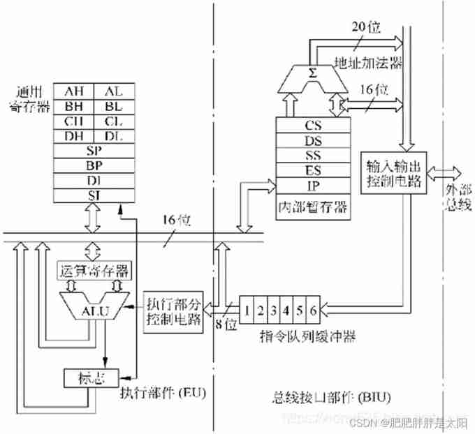
8086 Microprocessor (CPU) The composition of the

8086 Microprocessor is mainly composed of arithmetic unit ( Arithmetical logic unit ALU、 Address adders )、 controller ( Bus controller )、 Internal register group (14 Internal registers ) Three parts .
CPU Functionally, it is divided into execution units EU And bus interface unit BIU, The execution unit EU Responsible for the execution of instructions ; And the bus interface unit BIU Responsible for communication with memory and I/O Data transfer operation between interfaces . The specific term , Finish fetching instructions and sending them to the instruction queue , Cooperate with the action of the executing part , From a memory unit or I/O Port fetch operand , Or send the operation result to the memory unit or I/O port .
EU and BIU The working logic of is as follows :
① whenever 8086 There are two empty bytes in the instruction queue of , or BIU The instruction will be automatically fetched into the instruction queue . The order in which the instruction is taken is the order in which the instruction appears in the program ;
② whenever EU When preparing to execute an instruction , It will be from BIU Take out the code of the instruction at the front of the instruction queue of the component , Then it takes several clock cycles to execute the instructions . In the process of executing instructions , If you have to access memory or I/O port , that EU Will request BIU, Enter bus cycle , Finish accessing memory or I/O Port operation ; If at this time BIU Just in an idle state , Will respond immediately EU Bus request for . Such as BIU Fetching an instruction byte into the instruction queue , be BIU The bus cycle of this fetch instruction will be completed first , And then respond EU A request to access the bus .
③ When the instruction queue is full , And EU When there is no bus access request ,BIU It enters the idle state .④ Executing a branch instruction 、 When calling and returning instructions , Because the order of instructions to be executed has changed , The loaded bytes in the instruction queue are automatically eliminated ,BIU It will then load the instruction code in another program segment that is being redirected into the instruction queue .
From the above BIU And EU Action management principles of , It's not hard to see. , Their work is not synchronized , It is this relationship that is both independent and cooperative , bring 8086 You can execute instructions at the same time , Perform the operation of fetching instruction code , in other words BIU And EU Is a way of working in parallel , It changes the previous computer instruction fetching → decoding → Serial operation mode of executing instructions , It greatly improves the working efficiency , That's exactly what it is. 8086 One of the reasons for success .
Bus timing
CPU The bus timing of each pin of indicates the logical relationship of each pin , A bus cycle consists of four clock cycles , In one bus cycle CPU Finished reading / The operation of writing to memory ( Including output access address and read / write data ), The timing diagram of a clock cycle is as follows :

stay T1 moment , The working sequence of each pin is interpreted as follows :
CLK | Clock signal | High active |
A19/S6-A16/S3 | Bit19-bit16 Address signal | Address signal |
A15-A8 | Bit15-bit8 Address signal | Address signal |
AD7-AD0 | Bit7-bit0 Address signal | Address signal |
ALE | Address latch signal | High active |
IO/#M | Interface / Memory access control bit | # Indicates low level access to memory |
#RD | Read data operation enable signal | High level invalid |
DT/#R | Data access direction control bit | Low level allows data read operation |
#DEN | Allow data to read and write signals | High level allows access to data |
from Above 9 Group pin at T1 Time sequence and signal validity can be known “T1 What is executed at all times is Address output operation “.
Be careful :
1. A19/S6-A16/S3 These four pins are bit19-bit16 The upper four addresses and bit6-bit3 Multiplexing pin of status signal , Multi pin signal validity discrimination :

2. Address latch signal ALE The meaning is as follows :

In the figure ,DT/#R and #DEN Signals are signals for data transmission and reception .
3. about 8086 and 8088 For microprocessors IO Interface / Memory access flag bit validity is different :
8088 Microprocessor | IO/#M |
8086 Microprocessor | #IO/M |
4. Data sending and receiving methods are divided into “ Sync ( Just send the data )”,“ Half a synchronous ( Before sending and receiving data , First determine the status of the other party, and then conduct synchronous data transmission )”,“ asynchronous ( After sending 1byte The data will stop and wait for the other party's response )”. The difference between semi synchronous and asynchronous is : Semi synchronization means that each time the other party's status is detected, it will Transmit once , Induction is Per send 1byte Count I stopped to wait for the other party's reply .
stay T1 moment , The working sequence of each pin is interpreted as follows :
CLK | Clock signal | High active |
A19/S6-A16/S3 | Bit6-bit3 Status signals | Status signals |
AD7-AD0 | Bit7-bit0 Data signals | Data signals |
ALE | Address latch signal | Low level invalid |
IO/#M | Interface / Memory access control bit | # Indicates low level access to memory |
#RD | Read data operation enable signal | Low level active |
DT/#R | Data access direction control bit | Low level data read operation |
#DEN | Allow data to read and write signals | Low level allows read operation |
Be careful : because 8088 The input and output of microprocessor data are 8 Bit width bus structure and T2 moment CPU In read data state , therefore A15-A8 Signals are useless .
Bus classification
The bus is classified according to the type of transmission signal : data bus DB、 Address bus AB、 Control bus CB:
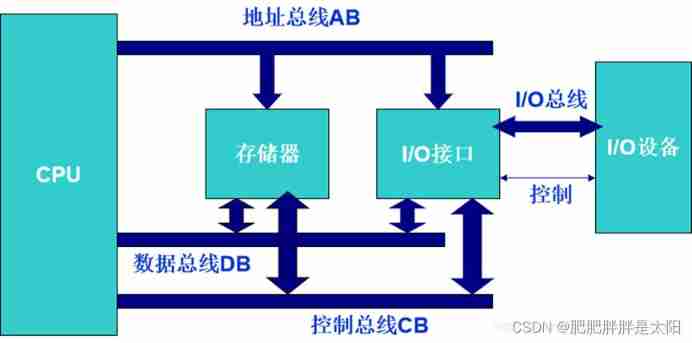
The bus is classified according to the structure hierarchy :
1. CPU Bus (CPU Internal bus )

2. The system bus (CPU Bus to interface )

3. External bus ( Interface to peripheral bus )
Bus structure
1. Single bus structure :

We know that memory has no other operation than storing data , therefore CPU The maximum speed of accessing memory is much higher than that of accessing IO The speed of the interface ( such as DAC Such peripherals , Its running speed is generally the highest 14MHz But the speed of memory access can reach hundreds of MHz). Low speed equipment and high-speed equipment share the same channel, which limits CPU Speed of accessing high-speed devices , therefore CPU The speed of accessing the bus is certain, and it is impossible to change back and forth according to the access device .
2. Dual bus structure :
① Memory and IO There is no direct channel between interfaces :

Although this structure can make high-speed devices access at high speed , Low speed devices are accessed at low speeds , But when our peripherals pass I/O When the port accesses the storage, it must go through CPU, As long as the access process passes through CPU The access speed will inevitably drop and give CPU Causing great pressure on data transmission .
② Memory and IO There are direct channels between interfaces :

At this time, high-speed devices can not only use high-speed access , Low speed devices use low-speed access and peripherals can access memory directly , This avoids CPU Only do the useless work of transmitting data , This is also the rudiment of our current multi bus architecture , We call this external device through IO The bus and controller for the port to directly access the memory are DMA(direct memory access).
3. Multi bus structure

The significance of bus and bus controller
1. As the transmission channel of signals, the bus must have enough Bus driver Ability and The data transfer Ability
Bus drive capability : Reflected by the operating frequency of the bus , The higher the operating frequency of the bus, the faster the data transmission speed ;
Data transmission capability : It is reflected by the bit width of the bus , The wider the bit width of the bus, the higher the transmission speed bit The more the number of . We can make the following analogy between the operating frequency of the bus and the bit width of the bus :
The operating frequency of the bus | Hz | The speed of a vehicle in a vehicle lane |
The bit width of the bus | Bit | The width of the car lane |
Bandwidth of the bus | Bps( Number of bits transmitted per second ) | The traffic volume per unit time of the car lane |
Let's consider that the longer the data length transmitted on the bus, the faster the transmission speed , Then the bus transmits... Per second bit The more , Therefore, the working frequency of the bus and the bit width of the bus determine the bandwidth of the bus :

2. Bus as CPU With multiple external devices / Multiple storage connected channels must have “ When there are multiple requests to occupy the bus , To be arbitrated “ The ability of
The basis for arbitration is nothing more than “ Priority of the device “ as well as ” The chronological order in which requests are published “.
3. As a channel for information transmission, the bus inevitably has transmission errors , here The bus must detect errors and handle them
边栏推荐
- 五、EL 表达式& JSTL 标签库
- Planning and design of 1000 person medium-sized campus / enterprise network based on ENSP and firewall (with all configuration commands)
- Database syntax related problems, solve a correct syntax
- Leetcode: offer 60 Points of N dice [math + level DP + cumulative contribution]
- LVDS drive adapter
- MySQL multiple SQL batch operations (crud) in JDBC
- Cron expression and website generation
- CL210OpenStack操作的故障排除--章节实验
- 8. 表单标签
- descheduler 二次调度让 Kubernetes 负载更均衡
猜你喜欢

SQL Server 2019 installation error. How to solve it

CL210OpenStack操作的故障排除--章节实验
![[data clustering] data set, visualization and precautions are involved in this column](/img/46/0b4918ef9c9301fbc374913fe806de.png)
[data clustering] data set, visualization and precautions are involved in this column

Installation and use of eigen under vs2017
最近面了15个人,发现这个测试基础题都答不上来...

RT thread studio learning (VII) using multiple serial ports
"I was laid off by a big factory"

Node, topic, parameter renaming and global, relative and private namespaces in ROS (example + code)

Curry carries the fourth game of the warriors against the Celtics
库里扛起了勇士对凯尔特人的第四场
随机推荐
TypeScript基础知识全集
paddlepaddl 28 支持任意维度数据的梯度平衡机制GHM Loss的实现(支持ignore_index、class_weight,支持反向传播训练,支持多分类)
sql server 2019安装出现错误,如何解决
循环链表和双向链表—课上课后练
ConVIRT论文详解(医疗图片)
Leetcode: Sword finger offer 63 Maximum profit of stock [record prefix minimum and or no brain segment tree]
leetcode:剑指 Offer 63. 股票的最大利润【记录前缀最小和 or 无脑线段树】
Idea common shortcut keys
Drawing grid navigation by opencv map reading
The most understandable explanation of coordinate transformation (push to + diagram)
Host computer development (firmware download software requirement analysis)
8. 表单标签
【高考那些事】准大学生看过来,选择方向和未来,自己把握
Freshmen are worried about whether to get a low salary of more than 10000 yuan from Huawei or a high salary of more than 20000 yuan from the Internet
Talk about vscode configuration settings JSON knows why (with a large number of configurations)
五、EL 表达式& JSTL 标签库
推荐17个提升开发效率的“轮子”
Circular linked list and bidirectional linked list - practice after class
Vscode Common plug - in
Zhang Chi's class: Notice on the time of CAQ Six Sigma test in 2022