当前位置:网站首页>Xpt2046 four wire resistive touch screen
Xpt2046 four wire resistive touch screen
2022-07-02 15:45:00 【Bitongo】
List of articles
One 、 brief introduction
XPT2046 Four wire resistive touch screen , It is mainly plated with ITO Film composition of the coating . One layer has a vertical bus on the left and right edges of the screen , The other layer has a horizontal bus at the bottom and top of the screen , If voltage is applied to two buses of a thin film , stay ITO A uniform electric field will be formed on the coating . When the user touches the touch screen , At the point of contact, two layers of film will contact , The voltage at the contact point can be measured on another layer of film .
The following figure for XPT2046 Functional block diagram , so XPT2046 There is a multiplexer inside , Able to measure battery voltage 、AUX voltage 、 Chip temperature . One 12 Bit ADC Used for analog-to-digital conversion of the selected analog input channel , Get the digital quantity , Then it is sent to the control logic circuit , For master control CPU To read , meanwhile , Which channel to choose for conversion , It is also controlled by the master CPU Send commands to the control logic to set .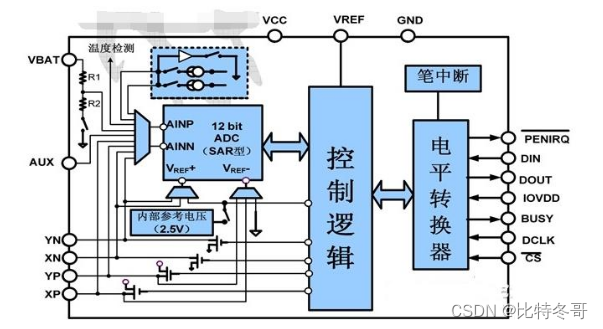
XPT Support stroke interruption , That is, when the touch screen detects that the touch is pressed , It can immediately produce stroke interruption , Inform the main controller that it can control the start of conversion and read data . In the process of transformation , adopt busy The signal indicates the current busy state , To avoid the master sending a new command to interrupt the previous command .
Two 、 Pins and their functions
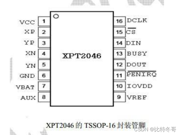

XPT2046 adopt SPI Interface communicates with the main controller , Its interface with the main controller includes the following signals :
PENIRQ_N: Stroke interrupt signal , When the stroke interrupt signal is set to be valid , Whenever the touch screen is pressed , This pin is pulled low . When the main control detects the signal , You can send a control signal to prohibit the interruption of strokes , So as to avoid triggering the controller interrupt by mistake in the conversion process . This pin is internally connected with a 50K The pull-up resistance of .
CS_N: Chip select signal , When CS_N When pulled down , It is used to control the conversion sequence and enable serial input / Output registers to move data out or in . When this pin is high , chip (ADC) Enter power down mode .
DCLK: External clock input , This clock is used to drive SARADC And drive numbers IO Serial data transmission on .
DIN: The data serial input pin of the chip , When CS Low power level , The data is on the serial clock DCLK The rising edge of is latched to the on-chip register .
DOUT: Serial data output , In the serial clock DCLK The falling edge data of is moved out of this pin , When CS_N Pin is high power level , This pin is in high resistance state .
BUSY: Busy output signal , When the chip receives the command and starts the conversion , This pin generates a DCLK High level of cycle . When the pin changes from high level to low level , The highest data of the conversion result is shown in DOUT On the pin , The master can read DOUT Value . When CS_N Pin is high power level ,BUSY Pin is in high resistance state .
3、 ... and 、 working principle
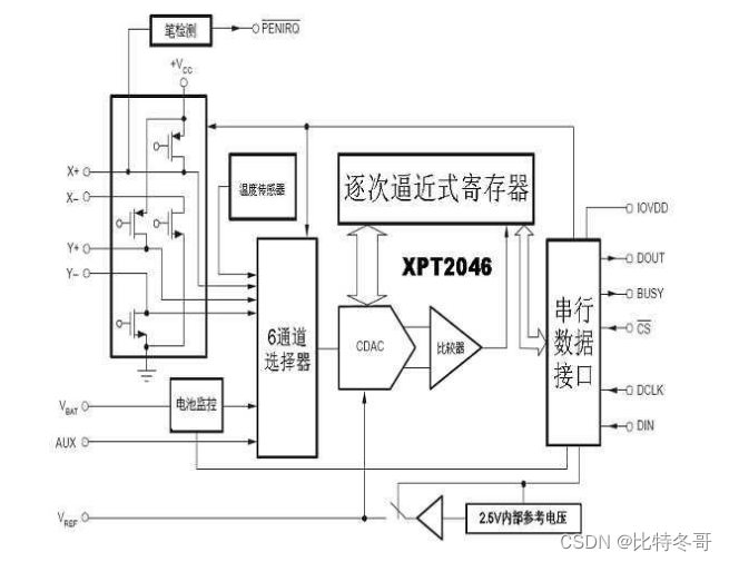
XPT2046 It is a typical successive approximation analog-to-digital converter (SARADC), Including sampling / keep 、 A / D conversion 、 Serial port data output and other functions . At the same time, the chip integrates a 2.5V Internal reference voltage source 、 Temperature detection circuit , Use external clock when working .XPT2046 It can be powered by a single power supply , The power supply voltage range is 2.7V~5.5V. The reference voltage value is directly determined ADC Input range of , The reference voltage can use an internal reference voltage , You can also input directly from the outside 1V~VCC Reference voltage in the range ( Low output impedance of external reference voltage source is required ).X、Y、Z、VBAT、Temp and AUX The analog signal enters after being selected by the on-chip control register ADC,ADC It can be configured as single ended or differential mode . choice VBAT、Temp and AUX It can be configured as single ended mode ; As a touch screen application , It can be configured as differential mode , This can effectively eliminate the measurement error caused by parasitic resistance of driving switch and external interference , Improve conversion accuracy .
The following figure for XPT2046 Typical working circuit :
XPT2046 There are four pins , For connecting to a four wire resistive screen FPC On , Respectively XP、XN、YP、YN, Connected to the corresponding four wire resistance screen X The positive end of the electrode 、 Negative end and Y The positive end of the electrode 、 Negative end . Each of these four pins can work in two states , They are power supply /GND Output 、ADC Input . For example setting ADC Working in differential mode , When measuring X Coordinate of direction ,XP Output VCC、XN Connect to GND, here ,YP and YN As ADC The differential input pin of is connected to ADC On , By measuring YP and YN To get the current touch point X Location . Empathy , When measuring Y Coordinate of direction ,YP Output VCC、YN Connect to GND、 here ,XN and XP As ADC The differential input pin of is connected to ADC On , By measuring YP and YN To get the current touch point Y Location .
Four 、 internal structure
5、 ... and 、 Function and use
Typical applications :
24 Clock cycle conversion
Read write timing
I understand XPT2046 The interface circuit , Then we can control MCU or FPGA To control the chip to read the coordinates . To read correctly X、Y coordinate , It is necessary to read and write data according to the control protocol specified by the chip .XPT2046 Make it happen once X、Y The reading of coordinates requires two transformations , A single conversion can only get a single X or Y Coordinates of , therefore , We have to control twice to get the result . The object of each conversion is X or Y coordinate , Determined by the control word sent by the controller .ADC It can be configured as single ended or differential mode during conversion , The specific control word is at the beginning of each transmission , Controlled by master MCU drive DIN Signal transmission . The following figure for XPT2046 Typical 24 Clock cycle conversion control timing :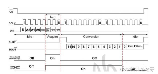
XPT2046 The data interface is a serial interface , Its typical working sequence is shown in the figure above , The signal shown in the figure comes from a single chip microcomputer or data signal processor with a basic serial interface . Communication between the processor and the converter requires 8 Clock cycles , May adopt SPI、SSI and Microwire Isochronous serial interface . A complete transformation requires 24 A serial synchronization clock (DCLK) To complete .
front 8 A clock is used to pass DIN Pin input control byte . When the converter gets enough information about the next conversion , Then, the input multiplexer and the reference source input are set according to the obtained information , And enter the sampling mode , if necessary , The touch panel drive will start .3 After several clock cycles , Control byte setting is complete , The converter enters the conversion state . At this time , Input sampling - The holder enters the hold state , The touch panel driver stops working ( Single ended operating mode ). And then 12 A clock cycle will complete the real analog-to-digital conversion . If it is a measurement ratio conversion method (SER/DFR——=0), The drive will work all the time during the conversion , The first 13 A clock will output the last bit of the conversion result . The rest 3 Multiple clock cycles will be used to complete the last byte ignored by the converter (DOUT Buy low ).
6、 ... and 、 Sample code
XPT2046 Read AD value
unsigned int XPT2046_ReadAD(unsigned char Command)
{

	unsigned char i;
	unsigned int Data=0;
	XPY2046_DCLK=0;
	XPY2046_CS=0;
	for(i=0;i<8;i++)
	{

		XPY2046_DIN=Command&(0x80>>i);
		XPY2046_DCLK=1;
		XPY2046_DCLK=0;
	}
	for(i=0;i<16;i++)
	{

		XPY2046_DCLK=1;
		XPY2046_DCLK=0;
		if(XPY2046_DOUT){
    Data|=(0x8000>>i);}
	}
	XPY2046_CS=1;
	return Data>>8;
}
边栏推荐
猜你喜欢
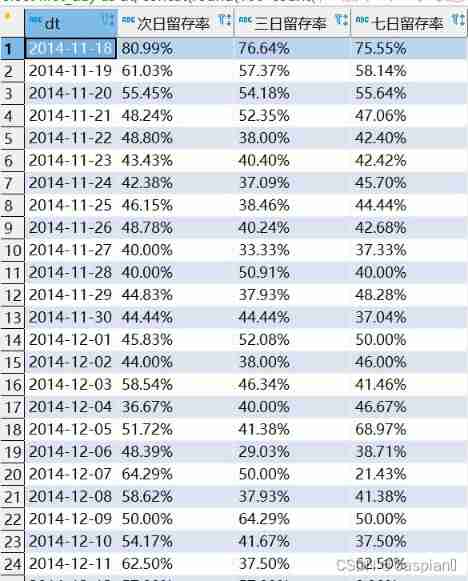
MySQL calculate n-day retention rate
Bing.com网站

Aiko ai Frontier promotion (7.2)
![[development environment] install Visual Studio Ultimate 2013 development environment (download software | install software | run software)](/img/26/3f19d36c048e669c736e27384e0fa7.jpg)
[development environment] install Visual Studio Ultimate 2013 development environment (download software | install software | run software)

PHP static members

Party History Documentary theme public welfare digital cultural and creative products officially launched

Why does the system convert the temp environment variable to a short file name?
(Video + graphic) machine learning introduction series - Chapter 5 machine learning practice
Soul torture, what is AQS???

Pytoch saves tensor to Mat file
随机推荐
Party History Documentary theme public welfare digital cultural and creative products officially launched
6096. 咒语和药水的成功对数
已知兩種遍曆序列構造二叉樹
【idea】推荐一个idea翻译插件:Translation「建议收藏」
Why does the system convert the temp environment variable to a short file name?
[leetcode] 695 - maximum area of the island
matlab中wavedec2,说说wavedec2函数[通俗易懂]
6.12 critical moment of Unified Process Platform
Leetcode question brushing - parity linked list 328 medium
【LeetCode】1162-地图分析
[leetcode] 876 intermediate node of linked list
动态规划入门二(5.647.62)
蚂蚁集团大规模图计算系统TuGraph通过国家级评测
夏季高考文化成绩一分一段表
For the problem that Folium map cannot be displayed, the temporary solution is as follows
制作p12证书[通俗易懂]
自定义异常
Some problems about pytorch extension
How to intercept the value of a key from the JSON string returned by wechat?
Golang MD5 encryption and MD5 salt value encryption