当前位置:网站首页>[write CPU by yourself] implementation of exception related instructions
[write CPU by yourself] implementation of exception related instructions
2022-06-22 06:30:00 【Abaabaababa】
MIPS Exception types defined in the schema
MIPS32 Architecture , Some things interrupt the normal execution process of the program , These things are called interrupt 、 trap 、 System calls and other interruptions in the process of program execution , Collectively referred to as exceptions .


Here OpenMIPS The processor only implements 6 Handling of exceptions in :
- Hardware reset
- interrupt ( Soft interrupt 、 Hard interrupt )
- syscall system call
- Invalid instructions
- overflow
- Exception thrown by self trapping instruction
After the exception , Enter the exception handling routine for specific processing , After processing , Return to the state before the exception and continue to execute .` Hardware reset is a special exception , It is not necessary to return from the exception handling routine , There is no need to protect the site , No need to save the return address , The treatment here is simple and crude : Clear all registers , From address 0x0 Processing instruction execution , It's reset . So this disposal details other 5 An exception handling process .
Precise anomaly
When an exception occurs , The sequential execution of the system will be interrupted , here , Several instructions are in different stages of the pipeline , The processor goes to the exception handling routine , After exception handling, return to the original program to continue execution . When an exception occurs , Because you don't want the exception handling routine to destroy the normal execution of the original program , For instructions that have not been executed , You must remember which stage of the assembly line it is in , So that execution can be resumed after exception handling , This is the exact exception
When an exception occurs , An instruction that is interrupted by an exception is called Abnormal victim , All the instructions preceding this instruction must be executed to the last stage of the pipeline , I.e. normal completion . However, the instruction and the instructions after the instruction must be cancelled .
for example
e.g.1

The second order add An overflow exception occurred during execution , under these circumstances , Instructions 1ori The instructions will be successfully completed , Instructions 2,3,4 Will be canceled . In order to achieve precise exception , The order in which exceptions occur must be the same as the order of instructions . On a pipeline processor , Exceptions occur at different stages of the pipeline , Bring problems .
e.g.2
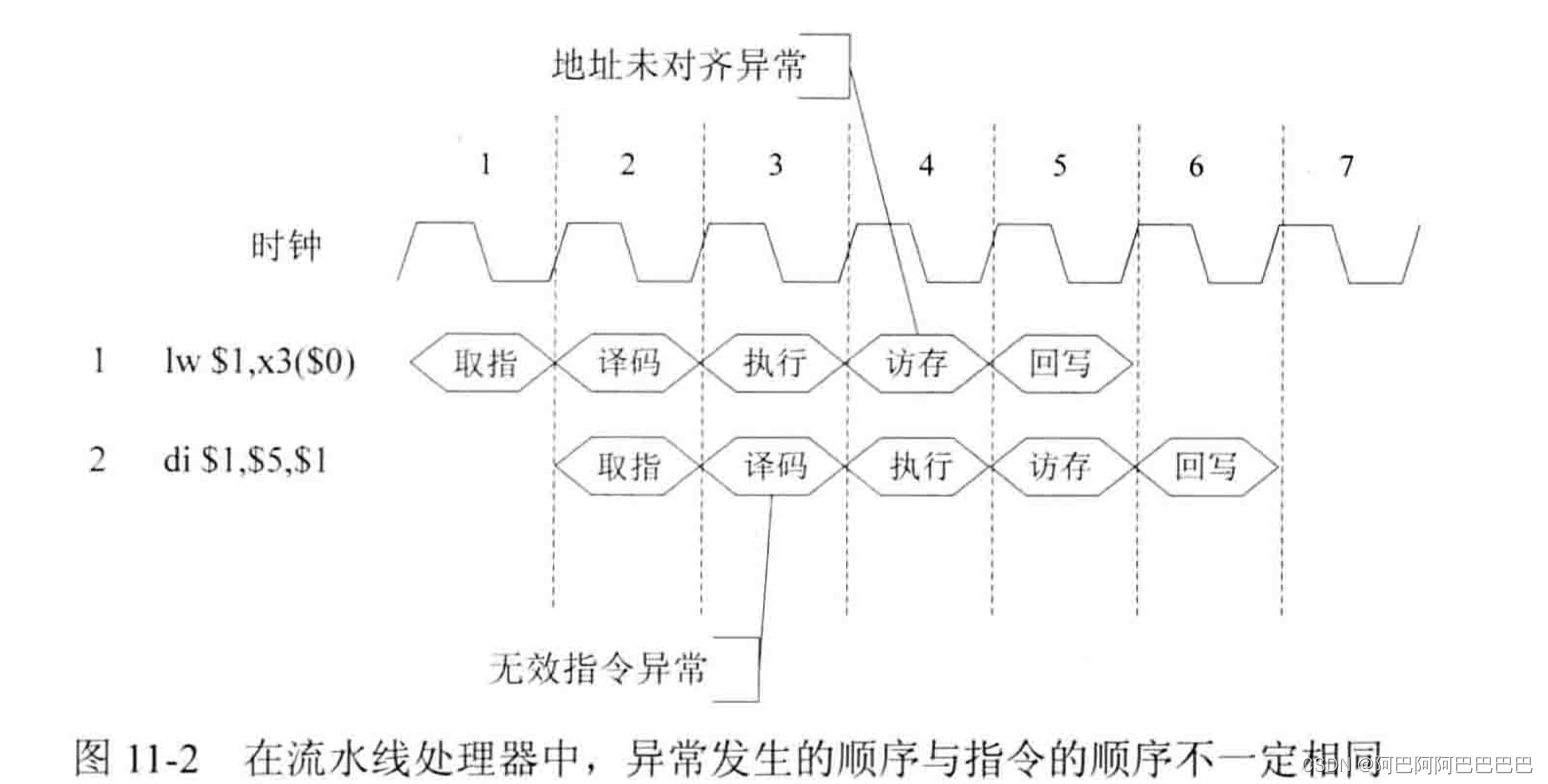
Load instruction lw An address misaligned exception will occur during the memory access phase of the pipeline , The exception will occur in the Four Clock cycles occur , The latter instruction di Is an invalid instruction mips32 Architecture does not have this directive , So it's invalid , An invalid instruction exception is thrown in the pipeline stage , That is the first. 3、 ... and A cycle , here Last load instruction lw It is still in the implementation stage , Not entering the deposit access stage , So the first exception that occurs is an invalid instruction exception . thus The order in which the unsatisfied exception occurs is the same as that of the instruction This requirement .
in order to avoid foregoing circumstances , Exceptions that occur first are not handled immediately , The exception event is simply marked , And continue to run the pipeline , In most processors , Meeting Design a special pipeline stage , Dedicated to handling exceptions , If The exception event of an instruction reaches this stage of the pipeline , Will be Do exception handling , And the exception events of the instructions currently in the rest of the pipeline will be Ignore .
Pictured above is an example , Assume that the processor will be in Handle exceptions in the storage access phase , that di The instruction is abnormal in the third cycle , But not Don't deal with , Just one. Save an exception tag , Wait to In the fifth clock cycle, the instruction will be processed when it enters the memory access phase . But in The fourth clock cycle , The last instruction lw Enter the deposit access stage , and Address misaligned exception occurred , Because it is already in In the stage of visit and deposit , So will Handle the exception , Include Exceptions in the rest of the pipeline, including invalid instruction exceptions, are ignored .
By the above methods , Implementation in pipeline processor Handle exceptions in the order they are executed , Instead of handling exceptions in the order they occur .
Exception handling
EXL by 1, It indicates that it is currently in the process of exception handling , If the current exception type is interrupt , So don't deal with , Ignore , Because interrupts are forbidden during exception handling . If the current exception type is not interrupt , Then save the exception reason to CP0 Medium Cause The register of ExCode Field
If EXL by 0, that Save the exception cause to CP0 Medium Cause The register of ExCode Field , Go to step two
Check occurrence Whether the abnormal instruction is in the delay slot , If in the delay slot , Then set EPC The value of the register is the address of the instruction minus 4, Simultaneous setting Cause The register of BD Field is 1, conversely , Set up EPC The value of the register is at the address of the instruction , Simultaneous setting Cause The register of BD Field is 0.
Set up Status register EXL Field is 1, Express Enter the exception handling process , No interruptions
The processor is transferred to A predefined address , In that address there are often Exception handling routine , Exception handling in it , This address is called Enter address for exception handling routine OpenMIPS The defined exception handling routine entry address table is as follows . Here is the system call 、 Invalid instructions 、 overflow 、 The four types of self trapping exceptions are all set to the same processing routine entry address , It can also be set to different addresses .
Specific exception handling will be performed in the exception handling routine , After processing , You need to return to the state before the exception to continue execution . Exception return instruction eret To finish the work ,eret The command should be cleared Status The register of EXL Field , So as to enable interruption , Try to make EPC The address saved in the register is restored to PC in , So as to return to the place where the exception occurred and continue to execute

After the delay slot is introduced , The order in which the processor executes the branch instructions :
Transfer order -> Delay slot instruction -> Transfer target instruction address
flow chart ( I am too lazy to draw )

Introduction to exception related instructions
Self trapping instruction
According to whether the instruction contains an immediate number , It is divided into 2 class
Self trapping instructions that do not contain immediate numbers
| 31-26 | 25-21 | 20-16 | 15-6 | 5-0 | useage | function |
|---|---|---|---|---|---|---|
| SPECIAL(000000) | rs | rt | code | TEQ(110100) | teq rs,rt | if GPR[rs]=GPR[rt] then trap Address is rs The value and address of the general-purpose register are rt Compare the values of the general-purpose registers of , If the two are equal , Self trapping exception occurs |
| SPECIAL(000000) | rs | rt | code | TGE(110000) | tge rs,rt | if GPR[rs] >= GPR[rt] then trap Address is rs The value and address of the general-purpose register are rt The value of a general-purpose register is compared as a signed number , If the former is greater than the latter , Then a self trapping exception is raised |
| SPECIAL(000000) | rs | rt | code | TGEU(110001) | tgeu rs,rt | if GPR[rs] >= GPR[rt] then trap Address is rs The value and address of the general-purpose register are rt The value of the general-purpose register of is used as nothing Symbol number comparison , If the former is greater than the latter , Then a self trapping exception is raised |
| SPECIAL(000000) | rs | rt | code | TLT(110010) | tlt rs,rt | if GPR[rs] < GPR[rt] then trap Address is rs The value and address of the general-purpose register are rt The value of a general-purpose register is compared as a signed number , If the former Small In the latter , Then a self trapping exception is raised |
| SPECIAL(000000) | rs | rt | code | TLTU(110011) | tltu rs,rt | if GPR[rs] >= GPR[rt] then trap Address is rs The value and address of the general-purpose register are rt The value of the general-purpose register of the nothing · Symbol number comparison , If the former Small In the latter , Then a self trapping exception is raised |
| SPECIAL(000000) | rs | rt | code | TNE(110110) | tne rs,rt | if GPR[rs] != GPR[rt] then trap Address is rs The value and address of the general-purpose register are rt Compare the values of the general-purpose registers of , If the two are not equal , Then a self trapping exception is raised |
A self trapping instruction containing an immediate number
| 31-26 | 25-21 | 20-16 | 15-0 | useage | function |
|---|---|---|---|---|---|
| REGIMM(000001) | rs | TEQI(01100) | immediate | teqi rs ,immediate | if GPR[rs]=sign_extended(immediate) then trap Address is rs The value of the general-purpose register and the instruction 16 The bit immediate sign is extended to 32 position Compare the values after , If the two are equal , That causes a self trapping anomaly |
| REGIMM(000001) | rs | TGEI(01000) | immediate | tgei rs ,immediate | if GPR[rs]=sign>=extended(immediate) then trap Address is rs The value of the general-purpose register and the instruction 16 The bit immediate sign is extended to 32 position Compare the values after , If the former is greater than or equal to the latter , Then a self trapping exception is raised |
| REGIMM(000001) | rs | TGEIU(01001) | immediate | tgeiu rs ,immediate | if GPR[rs]>=sign_extended(immediate) then trap Address is rs The value of the general-purpose register and the instruction 16 The bit immediate sign is extended to 32 The values after bits are compared as unsigned numbers , If the former is greater than or equal to the latter , Then a self trapping exception is raised |
| REGIMM(000001) | rs | TLTI(01010) | immediate | tlti rs ,immediate | if GPR[rs]<sign_extended(immediate) then trap Address is rs The value of the general-purpose register and the instruction 16 The bit immediate sign is extended to 32 The values after bits are compared as signed numbers , If the former is less than the latter , Then a self trapping exception is raised 、REGIMM(000001) |
| REGIMM(000001) | rs | TNEI(01110) | immediate | tnei rs ,immediate | if GPR[rs]!=sign_extended(immediate) then trap Address is rs The value of the general-purpose register and the instruction 16 The bit immediate sign is extended to 32 Compare the values after bits , If the two are not equal , Then a self trapping exception is raised |
Exception return instruction eret
| 31-26 | 25 | 24-6 | 5-0 | useage | function |
|---|---|---|---|---|---|
| COP0(010000) | CO(1) | 0000 0000 0000 0000 000 | ERET(011000) | eret | Returns... From the exception handling routine , Execute the command (1) yes EPC The value of the register is called the new fetch address (2) Set up Status The register of EXL Field is 0, Indicates that it is no longer at the exception level |
System call instructions syscall
| 31-26 | 25-6 | 5-0 | useage | function |
|---|---|---|---|---|
| SPECIAL(000000) | code | SYSCALL(001100) | syscall | System call exception thrown . Programs in user mode perform operations that can only be performed in kernel mode , You can call syscall Instructions , System call exception thrown , Enter the exception handling routine , So you can go into kernel mode |
Realize the idea
Mobile phone exception information at each stage of the assembly line , And pass it to the pipeline memory access stage , Handle the exception information at the same time in the memory access stage . Exception information to be collected at each stage of the pipeline :
decoding
Determine whether the system call is abnormal 、 Whether to return the instruction 、 Invalid instructions
perform
Judge whether there is self trapping anomaly 、 Overflow exception
Visiting and depositing
Check if there is any interruption . In the stage of visit and deposit , Processor combination CP0 The value of the relevant register in , Determine whether the exception needs to be handled , If you need to deal with , Then transfer to the entry address of the processing routine corresponding to the exception , Clear all information on the pipeline except the write back phase , Also modify the coprocessor CP0 The value of the relevant register in .eret Instructions , Transferred to the EPC At the address where the register is stored , At the same time, all information on the pipeline except the write back stage is cleared , Modify the coprocessor CP0 The value of the relevant register in . It is called clearing the information of a certain stage on the pipeline , In fact, you can set all the registers in this stage as initial values
Modification of data flow diagram

Determine the self trapping instruction 、syscall quality 、eret Instruction process
id
Modification of system structure
id
id The module determines whether to call the instruction syscall, Exception return instruction eret, Invalid instructions , Pass this information through excepttype_o Interface passed to ex modular , At the same time, the instruction address is passed through current_inst_addr_o The interface is passed to the execution phase .
ex
ex The module further determines whether there is a self trapping exception , Or overflow exception . This information will be integrated into id In the exception information of the module ,excepttype_i Pass in , adopt excepttype_o Pass on to mem modular . meanwhile current_inst_addr_o The interface passes the instruction address to mem modular , adopt is_delayslot_o Indicates whether the instruction is in the delay slot , This information will also be passed into mem modular .
mem
mem The module is based on the passed Exception types excepttype_i,Cause Register value cp0_cause_i,Status Register value cp0_status_i, Comprehensively judge whether to handle exceptions , If you need to deal with , The final exception type will skip excepttype_o The interface is sent to CTRL modular ,CTRL The module gives the entry address for exception handling new_pc Pass on to PC.
cp0_reg
When handling exceptions , Need modification CP0 Medium EPC,Status,Cause And so on , therefore mem The final exception type given by the module also needs to pass excepttype_o Interface feeding CP0 modular , Whether the abnormal command sent in at the same time is in the delay slot is_in_delayslot_i Interface feeding , The address of the exception instruction current_inst_address_o Interface feeding .CP0 The module modifies the value of the corresponding register according to this information .
CTRL
If you want to handle exceptions , It is necessary to clear the pipeline Writeback phase The value of the external register ,CTRL Modules are sent out by flush Realization .flush Module delivery PC,IF/ID,ID/EX,EX/MEM,MEM/WB Equal module , Set the registers in these modules as initial values .
LLbit
ll Set when executing LLbit by 1,sc Execution time , Check whether the register is 1, If 1 Just run normally , If 0, It indicates that there is interference , No storage operation . One of the causes of interference is ll,sc An exception occurred between the instructions , Therefore, one more step will be taken in the process of exception handling , take LLbit Register set to 0.
Code
Because it was written by myself cpu The last chapter of the Basic Edition , So put the complete code up .
pc_reg.v
`include "define.v"
module pc_reg(
input	wire										clk,
	input wire										rst,

	// Information from the control module
	input wire[5:0]               stall,
	input wire                    flush,
	input wire[`RegBus]           new_pc,

	// Information from the decoding phase
	input wire                    branch_flag_i,
	input wire[`RegBus]           branch_target_address_i,

	output reg[`InstAddrBus]			pc,
	output reg                    ce

);


always @ (posedge clk) begin
		if (rst == `RstEnable) begin
			ce <= `ChipDisable;
		end else begin
			ce <= `ChipEnable;
		end
	end


	/*always @ (posedge clk) begin if (ce == `ChipDisable) begin pc <= 32'h00000000; end else if(stall[0] == `NoStop)begin if(branch_flag_i == `Branch)begin// If a transfer occurs  pc <= branch_target_address_i;// Give the destination address of the transfer  end else begin pc <= pc + 4'h4; end end end*/

always @ (posedge clk)begin
	if(ce == `ChipDisable)begin
		pc <= 32'h00000000;
	end else begin
		if(flush == 1'b1)begin
			//flush==1 Indicates that an exception occurred   Will be taken from CTRL Exception handling given by the module
			// Routine entry address  new_pc Processing instruction execution
			pc <= new_pc;
		end else if(stall[0] == `NoStop)begin

			end
		end
	end
end
endmodule
inst_rom.v
`include "define.v"
//inst_rom.v
module inst_rom(
input wire ce,
input wire[`InstAddrBus] addr,
output reg[`InstBus] inst
);
// Define an array , Size is InstMemNum, The element width is InstBus
reg[`InstBus] inst_mem[0:`InstMemNum-1];
// Working with files inst_rom.data  Initialize instruction memory
initial $readmemh ("D:/test_2/inst_rom_11_3.data",inst_mem);
always @ (*)
begin
if(ce == `ChipDisable)// When the reset signal is invalid , According to the address entered , Give instruction memory ROM Corresponding elements in
begin
	inst <= `ZeroWord;
end
else begin
	inst <= inst_mem[addr[`InstMemNumLog2+1:2]];
end
end
endmodule
if_id.v
`include "define.v"
module if_id(

	input	wire										clk,
	input wire										rst,


	input wire[`InstAddrBus]			if_pc,
	input wire[`InstBus]          if_inst,
	input wire[5:0] stall, // Information from the control module
	input wire flush,
	output reg[`InstAddrBus]      id_pc,
	output reg[`InstBus]          id_inst

);
/************************** explain ****************************** *****stall[0] Indicates the fetch address PC Whether it remains the same , by 1 Keep the same ***** *******stall[1] Indicates whether the pipeline fetch phase is suspended , by 1 To suspend ******* *******stall[2] Indicates whether the pipeline decoding phase is suspended , by 1 To suspend ******* *******stall[3] Indicates whether the pipeline execution phase is suspended , by 1 To suspend ******* *******stall[4] Indicates whether the pipeline memory access phase is suspended , by 1 To suspend ******* *******stall[5] Indicates whether the pipeline write back phase is suspended , by 1 To suspend ******* (1)stall[1] by Stop,stall[5] by NoStop, Indicates that the fetch phase is suspended , Decoding stage   continue , Therefore, the null instruction is used as the instruction entering the decoding stage in the next cycle  (2)stall[1] by NoStop, The finger picking phase continues , The obtained instruction enters the decoding stage  (3) The rest of the time , Keep the register of decoding stage id_pc,id_inst unchanged  ************************************************************/

	always @ (posedge clk) begin
		if (rst == `RstEnable) begin
			id_pc <= `ZeroWord;
			id_inst <= `ZeroWord;
		end else if(flush== 1'b1)begin
			// Exception occurs   Clear the pipeline   So reset id_pc id_inst Register value
			id_pc <= `ZeroWord;
			id_inst <= `ZeroWord;
		end else if(stall[1] == `Stop && stall[2] == `NoStop)begin
			id_pc <= `ZeroWord;
			id_inst <= `ZeroWord;
		end else if(stall[1] == `NoStop)begin
			id_pc <= if_pc;
			id_inst <= if_inst;
		end
	end

endmodule
ctrl.v
//ctrl.v
`include "define.v"
module ctrl(
input wire rst,
input wire stallreq_from_id,
input wire stallreq_from_ex,
input wire[31:0] excepttype_i,
input wire[`RegBus] cp0_epc_i,
output reg[5:0] stall,
output reg[`RegBus] new_pc,
output reg flush
);
/************************** explain ****************************** *****stall[0] Indicates the fetch address PC Whether it remains the same , by 1 Keep the same ***** *******stall[1] Indicates whether the pipeline fetch phase is suspended , by 1 To suspend ******* *******stall[2] Indicates whether the pipeline decoding phase is suspended , by 1 To suspend ******* *******stall[3] Indicates whether the pipeline execution phase is suspended , by 1 To suspend ******* *******stall[4] Indicates whether the pipeline memory access phase is suspended , by 1 To suspend ******* *******stall[5] Indicates whether the pipeline write back phase is suspended , by 1 To suspend ******* ************************************************************/
always @ (*) begin
		if(rst == `RstEnable) begin
			stall <= 6'b000000;
			flush <= 1'b0;
			new_pc <= `ZeroWord;
		end else if(excepttype_i != `ZeroWord) begin
		  flush <= 1'b1;
		  stall <= 6'b000000;
			case (excepttype_i)
				32'h00000001:		begin   //interrupt
					new_pc <= 32'h00000020;
				end
				32'h00000008:		begin   //syscall
					new_pc <= 32'h00000040;
				end
				32'h0000000a:		begin   //inst_invalid
					new_pc <= 32'h00000040;
				end
				32'h0000000d:		begin   //trap
					new_pc <= 32'h00000040;
				end
				32'h0000000c:		begin   //ov
					new_pc <= 32'h00000040;
				end
				32'h0000000e:		begin   //eret
					new_pc <= cp0_epc_i;
				end
				default	: begin
				end
			endcase
		end else if(stallreq_from_ex == `Stop) begin
			stall <= 6'b001111;
			flush <= 1'b0;
		end else if(stallreq_from_id == `Stop) begin
			stall <= 6'b000111;
			flush <= 1'b0;
		end else begin
			stall <= 6'b000000;
			flush <= 1'b0;
			new_pc <= `ZeroWord;
		end    //if
	end      //always


endmodule
data_ram.v
`include "define.v"
module data_ram(
input wire clk,
input wire ce,// Data memory enable signal
input wire we,// Whether it is a write operation   Write 1
input wire[`DataAddrBus] addr,// Address to visit
input wire[3:0] sel,// Byte select signal
input wire[`DataBus] data_i,// The data to be written
output reg[`DataBus] data_o// Read out data
);


// Define a four byte array
reg[`ByteWidth] data_mem0[0:`DataMemNum-1];
reg[`ByteWidth] data_mem1[0:`DataMemNum-1];
reg[`ByteWidth] data_mem2[0:`DataMemNum-1];
reg[`ByteWidth] data_mem3[0:`DataMemNum-1];

// Write operations
always @ (posedge clk)begin
	if(ce == `ChipDisable) begin
	end else if(we == `WriteEnable)begin
		if(sel[3] == 1'b1)begin
			data_mem3[addr[`DataMemNumLog2+1:2]] <= data_i[31:24];
		end
		if(sel[2] == 1'b1)begin
			data_mem2[addr[`DataMemNumLog2+1:2]] <= data_i[23:16];
		end
		if(sel[1] == 1'b1)begin
			data_mem1[addr[`DataMemNumLog2+1:2]] <= data_i[15:8];
		end
		if(sel[0 == 1'b1])begin
			data_mem0[addr[`DataMemNumLog2+1:2]] <= data_i[7:0];
		end
	end
end

// Read operations
always @ (*) begin
	if(ce == `ChipDisable)begin
		data_o <= `ZeroWord;
	end else if(we == `WriteDisable)begin
		data_o <= {
    data_mem3[addr[`DataMemNumLog2+1:2]],data_mem2[addr[`DataMemNumLog2+1:2]],data_mem1[addr[`DataMemNumLog2+1:2]],data_mem0[addr[`DataMemNumLog2+1:2]]};
	end else begin
		data_o <= `ZeroWord;
	end
end
endmodule
define.v
// overall situation
`define RstEnable 1'b1
`define RstDisable 1'b0
`define ZeroWord 32'h00000000
`define WriteEnable 1'b1
`define WriteDisable 1'b0
`define ReadEnable 1'b1
`define ReadDisable 1'b0
`define AluOpBus 7:0
`define AluSelBus 2:0
`define InstValid 1'b0
`define InstInvalid 1'b1
`define Stop 1'b1
`define NoStop 1'b0
`define InDelaySlot 1'b1
`define NotInDelaySlot 1'b0
`define Branch 1'b1
`define NotBranch 1'b0
`define InterruputAssert 1'b1
`define InterruputNotAssert 1'b0
`define TrapAssert 1'b1
`define TrapNotAssert 1'b0
`define True_v 1'b1
`define False_v 1'b0
`define ChipEnable 1'b1
`define ChipDisable 1'b0


// Instructions
`define EXE_AND  6'b100100
`define EXE_OR   6'b100101
`define EXE_XOR 6'b100110
`define EXE_NOR 6'b100111
`define EXE_ANDI 6'b001100
`define EXE_ORI  6'b001101
`define EXE_XORI 6'b001110
`define EXE_LUI 6'b001111

`define EXE_SLL  6'b000000
`define EXE_SLLV  6'b000100
`define EXE_SRL  6'b000010
`define EXE_SRLV  6'b000110
`define EXE_SRA  6'b000011
`define EXE_SRAV  6'b000111
`define EXE_SYNC  6'b001111
`define EXE_PREF  6'b110011

`define EXE_MOVZ  6'b001010
`define EXE_MOVN  6'b001011
`define EXE_MFHI  6'b010000
`define EXE_MTHI  6'b010001
`define EXE_MFLO  6'b010010
`define EXE_MTLO  6'b010011

`define EXE_SLT  6'b101010
`define EXE_SLTU  6'b101011
`define EXE_SLTI  6'b001010
`define EXE_SLTIU  6'b001011
`define EXE_ADD  6'b100000
`define EXE_ADDU  6'b100001
`define EXE_SUB  6'b100010
`define EXE_SUBU  6'b100011
`define EXE_ADDI  6'b001000
`define EXE_ADDIU  6'b001001
`define EXE_CLZ  6'b100000
`define EXE_CLO  6'b100001

`define EXE_MULT  6'b011000
`define EXE_MULTU  6'b011001
`define EXE_MUL  6'b000010
`define EXE_MADD  6'b000000
`define EXE_MADDU  6'b000001
`define EXE_MSUB  6'b000100
`define EXE_MSUBU  6'b000101

`define EXE_DIV  6'b011010
`define EXE_DIVU  6'b011011

`define EXE_J  6'b000010
`define EXE_JAL  6'b000011
`define EXE_JALR  6'b001001
`define EXE_JR  6'b001000
`define EXE_BEQ  6'b000100
`define EXE_BGEZ  5'b00001
`define EXE_BGEZAL  5'b10001
`define EXE_BGTZ  6'b000111
`define EXE_BLEZ  6'b000110
`define EXE_BLTZ  5'b00000
`define EXE_BLTZAL  5'b10000
`define EXE_BNE  6'b000101

`define EXE_LB  6'b100000
`define EXE_LBU  6'b100100
`define EXE_LH  6'b100001
`define EXE_LHU  6'b100101
`define EXE_LL  6'b110000
`define EXE_LW  6'b100011
`define EXE_LWL  6'b100010
`define EXE_LWR  6'b100110
`define EXE_SB  6'b101000
`define EXE_SC  6'b111000
`define EXE_SH  6'b101001
`define EXE_SW  6'b101011
`define EXE_SWL  6'b101010
`define EXE_SWR  6'b101110

`define EXE_SYSCALL 6'b001100

`define EXE_TEQ 6'b110100
`define EXE_TEQI 5'b01100
`define EXE_TGE 6'b110000
`define EXE_TGEI 5'b01000
`define EXE_TGEIU 5'b01001
`define EXE_TGEU 6'b110001
`define EXE_TLT 6'b110010
`define EXE_TLTI 5'b01010
`define EXE_TLTIU 5'b01011
`define EXE_TLTU 6'b110011
`define EXE_TNE 6'b110110
`define EXE_TNEI 5'b01110

`define EXE_ERET 32'b01000010000000000000000000011000

`define EXE_NOP 6'b000000
`define SSNOP 32'b00000000000000000000000001000000

`define EXE_SPECIAL_INST 6'b000000
`define EXE_REGIMM_INST 6'b000001
`define EXE_SPECIAL2_INST 6'b011100

//AluOp
`define EXE_AND_OP   8'b00100100
`define EXE_OR_OP    8'b00100101
`define EXE_XOR_OP  8'b00100110
`define EXE_NOR_OP  8'b00100111
`define EXE_ANDI_OP  8'b01011001
`define EXE_ORI_OP  8'b01011010
`define EXE_XORI_OP  8'b01011011
`define EXE_LUI_OP  8'b01011100

`define EXE_SLL_OP  8'b01111100
`define EXE_SLLV_OP  8'b00000100
`define EXE_SRL_OP  8'b00000010
`define EXE_SRLV_OP  8'b00000110
`define EXE_SRA_OP  8'b00000011
`define EXE_SRAV_OP  8'b00000111

`define EXE_MOVZ_OP  8'b00001010
`define EXE_MOVN_OP  8'b00001011
`define EXE_MFHI_OP  8'b00010000
`define EXE_MTHI_OP  8'b00010001
`define EXE_MFLO_OP  8'b00010010
`define EXE_MTLO_OP  8'b00010011

`define EXE_SLT_OP  8'b00101010
`define EXE_SLTU_OP  8'b00101011
`define EXE_SLTI_OP  8'b01010111
`define EXE_SLTIU_OP  8'b01011000
`define EXE_ADD_OP  8'b00100000
`define EXE_ADDU_OP  8'b00100001
`define EXE_SUB_OP  8'b00100010
`define EXE_SUBU_OP  8'b00100011
`define EXE_ADDI_OP  8'b01010101
`define EXE_ADDIU_OP  8'b01010110
`define EXE_CLZ_OP  8'b10110000
`define EXE_CLO_OP  8'b10110001

`define EXE_MULT_OP  8'b00011000
`define EXE_MULTU_OP  8'b00011001
`define EXE_MUL_OP  8'b10101001
`define EXE_MADD_OP  8'b10100110
`define EXE_MADDU_OP  8'b10101000
`define EXE_MSUB_OP  8'b10101010
`define EXE_MSUBU_OP  8'b10101011

`define EXE_DIV_OP  8'b00011010
`define EXE_DIVU_OP  8'b00011011

`define EXE_J_OP  8'b01001111
`define EXE_JAL_OP  8'b01010000
`define EXE_JALR_OP  8'b00001001
`define EXE_JR_OP  8'b00001000
`define EXE_BEQ_OP  8'b01010001
`define EXE_BGEZ_OP  8'b01000001
`define EXE_BGEZAL_OP  8'b01001011
`define EXE_BGTZ_OP  8'b01010100
`define EXE_BLEZ_OP  8'b01010011
`define EXE_BLTZ_OP  8'b01000000
`define EXE_BLTZAL_OP  8'b01001010
`define EXE_BNE_OP  8'b01010010

`define EXE_LB_OP  8'b11100000
`define EXE_LBU_OP  8'b11100100
`define EXE_LH_OP  8'b11100001
`define EXE_LHU_OP  8'b11100101
`define EXE_LL_OP  8'b11110000
`define EXE_LW_OP  8'b11100011
`define EXE_LWL_OP  8'b11100010
`define EXE_LWR_OP  8'b11100110
`define EXE_PREF_OP  8'b11110011
`define EXE_SB_OP  8'b11101000
`define EXE_SC_OP  8'b11111000
`define EXE_SH_OP  8'b11101001
`define EXE_SW_OP  8'b11101011
`define EXE_SWL_OP  8'b11101010
`define EXE_SWR_OP  8'b11101110
`define EXE_SYNC_OP  8'b00001111

`define EXE_MFC0_OP 8'b01011101
`define EXE_MTC0_OP 8'b01100000

`define EXE_SYSCALL_OP 8'b00001100

`define EXE_TEQ_OP 8'b00110100
`define EXE_TEQI_OP 8'b01001000
`define EXE_TGE_OP 8'b00110000
`define EXE_TGEI_OP 8'b01000100
`define EXE_TGEIU_OP 8'b01000101
`define EXE_TGEU_OP 8'b00110001
`define EXE_TLT_OP 8'b00110010
`define EXE_TLTI_OP 8'b01000110
`define EXE_TLTIU_OP 8'b01000111
`define EXE_TLTU_OP 8'b00110011
`define EXE_TNE_OP 8'b00110110
`define EXE_TNEI_OP 8'b01001001

`define EXE_ERET_OP 8'b01101011

`define EXE_NOP_OP    8'b00000000

//AluSel
`define EXE_RES_LOGIC 3'b001
`define EXE_RES_SHIFT 3'b010
`define EXE_RES_MOVE 3'b011
`define EXE_RES_ARITHMETIC 3'b100
`define EXE_RES_MUL 3'b101
`define EXE_RES_JUMP_BRANCH 3'b110
`define EXE_RES_LOAD_STORE 3'b111

`define EXE_RES_NOP 3'b000


// Instruction memory inst_rom
`define InstAddrBus 31:0
`define InstBus 31:0
`define InstMemNum 131071
`define InstMemNumLog2 17

// Data storage data_ram
`define DataAddrBus 31:0
`define DataBus 31:0
`define DataMemNum 131071
`define DataMemNumLog2 17
`define ByteWidth 7:0

// General registers regfile
`define RegAddrBus 4:0
`define RegBus 31:0
`define RegWidth 32
`define DoubleRegWidth 64
`define DoubleRegBus 63:0
`define RegNum 32
`define RegNumLog2 5
`define NOPRegAddr 5'b00000

// division div
`define DivFree 2'b00
`define DivByZero 2'b01
`define DivOn 2'b10
`define DivEnd 2'b11
`define DivResultReady 1'b1
`define DivResultNotReady 1'b0
`define DivStart 1'b1
`define DivStop 1'b0

//CP0 Register address
`define CP0_REG_COUNT    5'b01001        // read-write
`define CP0_REG_COMPARE    5'b01011      // read-write
`define CP0_REG_STATUS    5'b01100       // read-write
`define CP0_REG_CAUSE    5'b01101        // read-only
`define CP0_REG_EPC    5'b01110          // read-write
`define CP0_REG_PrId    5'b01111         // read-only
`define CP0_REG_CONFIG    5'b10000       // read-only
div.v
`include "define.v"
module div(

	input	wire										clk,
	input wire										rst,

	input wire                    signed_div_i,
	input wire[31:0]              opdata1_i,
	input wire[31:0]		   				opdata2_i,
	input wire                    start_i,
	input wire                    annul_i,

	output reg[63:0]             result_o,
	output reg			             ready_o
);

	wire[32:0] div_temp;
	reg[5:0] cnt;
	reg[64:0] dividend;
	reg[1:0] state;
	reg[31:0] divisor;
	reg[31:0] temp_op1;
	reg[31:0] temp_op2;

	assign div_temp = {
    1'b0,dividend[63:32]} - {1'b0,divisor};

	always @ (posedge clk) begin
		if (rst == `RstEnable) begin
			state <= `DivFree;
			ready_o <= `DivResultNotReady;
			result_o <= {
    `ZeroWord,`ZeroWord};
		end else begin
		  case (state)
		  	`DivFree:			begin               //DivFree״̬
		  		if(start_i == `DivStart && annul_i == 1'b0) begin
		  			if(opdata2_i == `ZeroWord) begin
		  				state <= `DivByZero;
		  			end else begin
		  				state <= `DivOn;
		  				cnt <= 6'b000000;
		  				if(signed_div_i == 1'b1 && opdata1_i[31] == 1'b1 ) begin
		  					temp_op1 = ~opdata1_i + 1;
		  				end else begin
		  					temp_op1 = opdata1_i;
		  				end
		  				if(signed_div_i == 1'b1 && opdata2_i[31] == 1'b1 ) begin
		  					temp_op2 = ~opdata2_i + 1;
		  				end else begin
		  					temp_op2 = opdata2_i;
		  				end
		  				dividend <= {
    `ZeroWord,`ZeroWord};
              dividend[32:1] <= temp_op1;
              divisor <= temp_op2;
             end
          end else begin
						ready_o <= `DivResultNotReady;
						result_o <= {
    `ZeroWord,`ZeroWord};
				  end
		  	end
		  	`DivByZero:		begin               //DivByZero״̬
         	dividend <= {
    `ZeroWord,`ZeroWord};
          state <= `DivEnd;
		  	end
		  	`DivOn:				begin               //DivOn״̬
		  		if(annul_i == 1'b0) begin
		  			if(cnt != 6'b100000) begin
               if(div_temp[32] == 1'b1) begin
                  dividend <= {
    dividend[63:0] , 1'b0};
               end else begin
                  dividend <= {
    div_temp[31:0] , dividend[31:0] , 1'b1};
               end
               cnt <= cnt + 1;
             end else begin
               if((signed_div_i == 1'b1) && ((opdata1_i[31] ^ opdata2_i[31]) == 1'b1)) begin
                  dividend[31:0] <= (~dividend[31:0] + 1);
               end
               if((signed_div_i == 1'b1) && ((opdata1_i[31] ^ dividend[64]) == 1'b1)) begin
                  dividend[64:33] <= (~dividend[64:33] + 1);
               end
               state <= `DivEnd;
               cnt <= 6'b000000;
             end
		  		end else begin
		  			state <= `DivFree;
		  		end
		  	end
		  	`DivEnd:			begin               //DivEnd״̬
        	result_o <= {
    dividend[64:33], dividend[31:0]};
          ready_o <= `DivResultReady;
          if(start_i == `DivStop) begin
          	state <= `DivFree;
						ready_o <= `DivResultNotReady;
						result_o <= {
    `ZeroWord,`ZeroWord};
          end
		  	end
		  endcase
		end
	end

endmodule
id.v
`include "define.v"
module id(
input wire rst,
input wire[`InstAddrBus] pc_i,
input wire[`InstBus] inst_i,
input wire[`RegBus] reg1_data_i,
input wire[`RegBus] reg2_data_i,
input wire is_in_delayslot_i,// Whether it is in the delay slot instruction
// Deliver to regfile Information about
output reg reg1_read_o,
output reg reg2_read_o,
output reg[`RegAddrBus] reg1_addr_o,
output reg[`RegAddrBus] reg2_addr_o,
// Information sent to the execution phase
output reg[`AluOpBus] aluop_o,
output reg[`AluSelBus] alusel_o,
output reg[`RegBus] reg1_o,
output reg[`RegBus] reg2_o,
output reg[`RegAddrBus] wd_o,
output reg wreg_o,
// The operation result of the instruction in the execution stage
input wire ex_wreg_i,
input wire[`RegBus] ex_wdata_i,
input wire[`RegAddrBus] ex_wd_i,
input wire[`AluOpBus] ex_aluop_i,
// The operation result of the instruction in the memory access stage
input wire mem_wreg_i,
input wire[`RegBus] mem_wdata_i,
input wire[`RegAddrBus] mem_wd_i,
output wire stallreq,
output reg next_inst_in_delayslot_o,// Whether the next instruction is a delay slot
output reg branch_flag_o,// Whether there is a transfer
output reg[`RegBus] branch_target_address_o,// Transfer to destination address
output reg[`RegBus] link_addr_o,// The return address of the transfer instruction to be saved
output reg is_in_delayslot_o,// Whether the currently decoded instruction is in the delay slot
output wire[`RegBus] inst_o ,// Newly added output interface
//input wire[`AluOpBus] ex_aluop_i,
//output wire stallreq
output wire[31:0] excepttype_o,// Collected exception information
output wire[`RegBus] current_inst_address_o// The address of the decoding stage instruction
);
wire[5:0] op = inst_i[31:26];
wire[4:0] op2 = inst_i[10:6];
wire[5:0] op3 = inst_i[5:0];
wire[4:0] op4 = inst_i[20:16];
wire[`RegBus] pc_plus_8;// Save the address of the second instruction after the instruction in the current decoding stage
wire[`RegBus] pc_plus_4;// Save the instruction address immediately following the instruction in the current decoding stage
wire[`RegBus] imm_sll2_signedext;// In the corresponding branch instruction offset Move two places to the left , Then the symbol is extended to 32 The value of a
reg[`RegBus] imm;
reg instvalid;
reg excepttype_is_syscall;// Whether it is a system call exception syscall
reg excepttype_is_eret;// Whether it is an exception return instruction
/*excepttype_o The lower eight bits of are reserved for external interrupts , The eighth digit indicates whether it is syscall Caused by instructions System call exception , The ninth bit indicates whether the exception is caused by an invalid instruction , The twelfth digit indicates whether it is eret Instructions eret An instruction can be considered a special exception -- Return exception */
assign excepttype_o = {
19'b0,excepttype_is_eret,2'b0,instvalid,excepttype_is_syscall,8'b0};
// Input signal pc_i Is the address of the instruction currently in the decoding phase
assign current_inst_address_o = pc_i;
assign stallreq = `NoStop;// Loading in implementation 、 The signal is assigned a value when the instruction is stored
assign imm_sll2_signedext = {
{
14{
inst_i[15]}},inst_i[15:0],2'b00};
//imm_sll2_signedext Corresponding to... In branch instruction offset Move two places to the left , Then the symbol is extended to 32 The value of a
assign pc_plus_8 = pc_i+8;
assign pc_plus_4 = pc_i+4;
assign stallreq = `NoStop;
assign inst_o = inst_i;// Instructions in the decoding stage
// Define a new variable Indicates the register to be read 1 Whether it exists with the previous instruction load relevant
reg stallreq_for_reg1_loadrelate;
// Define a new variable Indicates the register to be read 2 Whether it exists with the previous instruction load relevant
reg stallreq_for_reg2_loadrelate;
// Define a new variable Indicates whether the previous instruction is a load instruction
wire pre_inst_is_load;
// According to the input signal ex_aluop_i value Determine whether the previous instruction is a load instruction
// If it's a load instruction So set pre_inst_is_load by 1 Reverse 0
assign pre_inst_is_load = ((ex_aluop_i == `EXE_LB_OP)||
(ex_aluop_i == `EXE_LBU_OP)||
(ex_aluop_i == `EXE_LH_OP)||
(ex_aluop_i==`EXE_LHU)||
(ex_aluop_i==`EXE_LW_OP)||
(ex_aluop_i==`EXE_LWR_OP)||
(ex_aluop_i==`EXE_LWL_OP)||
(ex_aluop_i==`EXE_LL_OP)||
(ex_aluop_i==`EXE_SC_OP)) ? 1'b1 : 1'b0;
/* If the last instruction is a load instruction And the loading instruction to be loaded into the destination register is the current instruction To pass the Regfile Module read port 1 Read the general register , Then it means that there is load relevant */
// Set up stallreq_for_reg1_loadrelate by Stop
always @(*)begin
stallreq_for_reg1_loadrelate <= `NoStop;
if(rst == `RstEnable)begin
reg1_o <= `ZeroWord;
end else if(pre_inst_is_load == 1'b1 && ex_wd_i == reg1_addr_o && reg1_read_o == 1'b1)begin
stallreq_for_reg1_loadrelate <= `Stop;// There is load relevant Stop
end
end
//reg2 And reg1 Empathy
always @(*)begin
stallreq_for_reg2_loadrelate <= `NoStop;
if(rst == `RstEnable)begin
reg2_o <= `ZeroWord;
end else if(pre_inst_is_load == 1'b1 && ex_wd_i == reg2_addr_o && reg2_read_o == 1'b1)begin
stallreq_for_reg2_loadrelate <= `Stop;// There is load relevant Stop
end
end
assign stallreq = stallreq_for_reg1_loadrelate | stallreq_for_reg2_loadrelate;
always @ (*) begin
if (rst == `RstEnable) begin
aluop_o <= `EXE_NOP_OP;
alusel_o <= `EXE_RES_NOP;//nop
wd_o <= `NOPRegAddr;
wreg_o <= `WriteDisable;
instvalid <= `InstValid;
reg1_read_o <= 1'b0;
reg2_read_o <= 1'b0;
reg1_addr_o <= `NOPRegAddr;
reg2_addr_o <= `NOPRegAddr;
imm <= 32'h0;
link_addr_o <= `ZeroWord;// The return address of the transfer instruction to be saved
branch_target_address_o <= `ZeroWord;// Transfer to destination address
branch_flag_o <= `NotBranch;// No transfer
next_inst_in_delayslot_o <= `NotInDelaySlot;// Whether the next instruction is in the delay slot
end else begin // Initialize first
aluop_o <= `EXE_NOP_OP;
alusel_o <= `EXE_RES_NOP;
wd_o <= inst_i[15:11];
wreg_o <= `WriteDisable;
instvalid <= `InstInvalid;
reg1_read_o <= 1'b0;
reg2_read_o <= 1'b0;
reg1_addr_o <= inst_i[25:21];//rs
reg2_addr_o <= inst_i[20:16];//rt
imm <= `ZeroWord;
link_addr_o <= `ZeroWord;
branch_target_address_o <= `ZeroWord;
branch_flag_o <= `NotBranch;
next_inst_in_delayslot_o <= `NotInDelaySlot;
excepttype_is_syscall <= `False_v;// There is no system call exception by default
excepttype_is_eret <= `False_v;// Default is not eret Instructions
instvalid <= `InstInvalid;// Default invalid directive
case (op)// Instruction code
`EXE_SPECIAL_INST: begin // The instruction code is SPECIAL
case(op2)// Function code
5'b00000: begin
case(op3) // Judge which instruction it is according to the function code
`EXE_OR: begin //or R Type command rs|rt -> rd
wreg_o <= `WriteEnable;
aluop_o <= `EXE_OR_OP;
alusel_o <= `EXE_RES_LOGIC;
reg1_read_o <= 1'b1;
reg2_read_o <= 1'b1;
instvalid <= `InstValid;
end
`EXE_AND:begin
wreg_o <= `WriteEnable;
aluop_o <= `EXE_AND_OP;//R rs&rt ->rd
alusel_o <= `EXE_RES_LOGIC;
reg1_read_o <= 1'b1;
reg2_read_o <= 1'b1;
instvalid <= `InstValid;
end
`EXE_XOR:begin
wreg_o <= `WriteEnable;
aluop_o <= `EXE_XOR_OP;// R rs^rt ->rd
alusel_o <= `EXE_RES_LOGIC;
reg1_read_o <= 1'b1;
reg2_read_o <= 1'b1;
instvalid <= `InstValid;
end
`EXE_NOR:begin
wreg_o <= `WriteEnable;
aluop_o <= `EXE_NOR_OP;// R rs~|rt ->rd
alusel_o <= `EXE_RES_LOGIC;
reg1_read_o <= 1'b1;
reg2_read_o <= 1'b1;
instvalid <= `InstValid;
end
`EXE_SLLV:begin
wreg_o <= `WriteEnable;
aluop_o <= `EXE_SLL_OP;
alusel_o <= `EXE_RES_SHIFT;
reg1_read_o <= 1'b1;
reg2_read_o <= 1'b1;
instvalid <= `InstValid;
end
`EXE_SRLV:begin
wreg_o <= `WriteEnable;
aluop_o <= `EXE_SRLV_OP;
alusel_o <= `EXE_RES_SHIFT;
reg1_read_o <= 1'b1;
reg2_read_o <= 1'b1;
instvalid <= `InstValid;
end
`EXE_SRAV:begin
wreg_o <= `WriteEnable;
aluop_o <= `EXE_SRAV_OP;
alusel_o <= `EXE_RES_SHIFT;
reg1_read_o <= 1'b1;
reg2_read_o <= 1'b1;
instvalid <= `InstValid;
end
`EXE_SYNC:begin
wreg_o <= `WriteEnable;
aluop_o <= `EXE_NOP_OP;
alusel_o <= `EXE_RES_NOP;
reg1_read_o <= 1'b0;
reg2_read_o <= 1'b1;
instvalid <= `InstValid;
end
`EXE_MFHI:begin// The special register hi The value of is assigned to the address rd The register of
wreg_o <= `WriteEnable;
aluop_o <= `EXE_MFHI_OP;
alusel_o <= `EXE_RES_MOVE;
reg1_read_o <= 1'b0;
reg2_read_o <= 1'b0;
instvalid <= `InstValid;
end
`EXE_MFLO:begin
wreg_o <= `WriteEnable;
aluop_o <= `EXE_MFLO_OP;
alusel_o <= `EXE_RES_MOVE;
reg1_read_o <= 1'b0;
reg2_read_o <= 1'b0;
instvalid <= `InstValid;
end
`EXE_MTHI:begin//hi<-rs Write special registers
wreg_o <= `WriteEnable;
aluop_o <= `EXE_MTHI_OP;
alusel_o <= `EXE_RES_MOVE;
reg1_read_o <= 1'b1;
reg2_read_o <= 1'b0;
instvalid <= `InstValid;
end
`EXE_MTLO:begin //lo<-rs Write special registers
wreg_o <= `WriteEnable;
aluop_o <= `EXE_MTLO_OP;
reg1_read_o <= 1'b1;//rs
reg2_read_o <= 1'b0;
instvalid <= `InstValid;
end
`EXE_MOVN:begin// Judge rt Register value If not for 0 take rs The value is assigned to rd conversely rd The value remains the same
//wreg_o <= `WriteEnable;
aluop_o <= `EXE_MOVN_OP;
alusel_o <= `EXE_RES_MOVE;
reg1_read_o <= 1'b1;
reg2_read_o <= 1'b1;
instvalid <= `InstValid;
//reg2_o The value of is the address rt The value of the register for
if(reg2_o != `ZeroWord)begin
wreg_o <= `WriteEnable;
end else begin
wreg_o <= `WriteDisable;
end
end
`EXE_MOVZ:begin // Judge rt Register value If it is 0 take rs The value is assigned to rd conversely rd The value remains the same
aluop_o <= `EXE_MOVZ_OP;
alusel_o <= `EXE_RES_MOVE;
reg1_read_o <= 1'b1;
reg2_read_o <= 1'b1;
instvalid <= `InstValid;
if(reg2_o == `ZeroWord)begin
wreg_o <= `WriteEnable;
end else begin
wreg_o <= `WriteDisable;
end
end
`EXE_SLT:begin//slt Instructions rd<-(rs<rt)
wreg_o <= `WriteEnable;
aluop_o <= `EXE_SLT_OP;
alusel_o <= `EXE_RES_ARITHMETIC;
reg1_read_o <= 1'b1;
reg2_read_o <= 1'b1;
instvalid <= `InstValid;
end
`EXE_SLTU:begin //sltu Instructions
wreg_o <= `WriteEnable;
aluop_o <= `EXE_SLTU_OP;
alusel_o <= `EXE_RES_ARITHMETIC;
reg1_read_o <= 1'b1;
reg2_read_o <= 1'b1;
instvalid <= `InstValid;
end
`EXE_ADD:begin//rd<-rs+rt
wreg_o <= `WriteEnable;
aluop_o <= `EXE_ADD_OP;
alusel_o <= `EXE_RES_ARITHMETIC;
reg1_read_o <= 1'b1;
reg2_read_o <= 1'b1;
instvalid <= `InstValid;
end
`EXE_ADDU:begin
wreg_o <= `WriteEnable;
aluop_o <= `EXE_ADDU_OP;
alusel_o <= `EXE_RES_ARITHMETIC;
reg1_read_o <= 1'b1;
reg2_read_o <= 1'b1;
instvalid <= `InstValid;
end
`EXE_SUB:begin
wreg_o <= `WriteEnable;
aluop_o <= `EXE_SUB_OP;
alusel_o <= `EXE_RES_ARITHMETIC;
reg1_read_o <= 1'b1;
reg2_read_o <= 1'b1;
instvalid <= `InstValid;
end
`EXE_SUBU:begin
wreg_o <= `WriteEnable;
aluop_o <= `EXE_SUBU_OP;
alusel_o <= `EXE_RES_ARITHMETIC;
reg1_read_o <= 1'b1;
reg2_read_o <= 1'b1;
instvalid <= `InstValid;
end
`EXE_MULT:begin
wreg_o <= `WriteEnable;
aluop_o <= `EXE_MULT_OP;
reg1_read_o <= 1'b1;
reg2_read_o <= 1'b1;
instvalid <= `InstValid;
end
`EXE_MULTU:begin
wreg_o <= `WriteEnable;
aluop_o <= `EXE_MULTU_OP;
reg1_read_o <= 1'b1;
reg2_read_o <= 1'b1;
instvalid <= `InstValid;
end
`EXE_DIV:begin
wreg_o <= `WriteDisable;
aluop_o <= `EXE_DIV_OP;
reg1_read_o <= 1'b1;
reg2_read_o <= 1'b1;
instvalid <= `InstValid;
end
`EXE_DIVU:begin
wreg_o <= `WriteDisable;
aluop_o <= `EXE_DIVU_OP;
reg1_read_o <= 1'b1;
reg2_read_o <= 1'b1;
instvalid <= `InstValid;
end
`EXE_JR:begin
wreg_o <= `WriteDisable;
aluop_o <= `EXE_JR_OP;
alusel_o <= `EXE_RES_JUMP_BRANCH;
reg1_read_o <= 1'b1;//rs Registers need to be used
reg2_read_o <= 1'b0;
wd_o <= inst_i[15:11];
link_addr_o <= pc_plus_8;// The return address
branch_target_address_o <= reg1_o;// Transfer to destination address
branch_flag_o <= `Branch;// Whether there is a transfer
next_inst_in_delayslot_o <= `InDelaySlot;// The next instruction is not in the delay slot
instvalid <= `InstValid;
end
`EXE_JALR:begin
wreg_o <= `WriteEnable;
aluop_o <= `EXE_JALR_OP;
alusel_o <= `EXE_RES_JUMP_BRANCH;
reg1_read_o <= 1'b1;
reg2_read_o <= 1'b0;
wd_o <= inst_i[15:11];
link_addr_o <= pc_plus_8;
branch_target_address_o <= reg1_o;
branch_flag_o <= `Branch;
next_inst_in_delayslot_o <= `InDelaySlot;
instvalid <= `InstValid;
end
`EXE_TEQ:begin//teq
wreg_o <= `WriteDisable;
aluop_o <= `EXE_SYSCALL_OP;
alusel_o <= `EXE_RES_NOP;
reg1_read_o <= 1'b0;
reg2_read_o <= 1'b0;
instvalid <= `InstValid;
end
`EXE_TGE:begin//tge
wreg_o <= `WriteDisable;
aluop_o <= `EXE_TGE_OP;
alusel_o <= `EXE_RES_NOP;
reg1_read_o <= 1'b1;
reg2_read_o <= 1'b1;
instvalid <= `InstValid;
end
`EXE_TGEU:begin//tgeu
wreg_o <= `WriteDisable;
aluop_o <= `EXE_TGEU_OP;
alusel_o <= `EXE_RES_NOP;
reg1_read_o <= 1'b1;
reg2_read_o <= 1'b1;
instvalid <= `InstValid;
end
`EXE_TLT:begin//tlt
wreg_o <= `WriteDisable;
aluop_o <= `EXE_TLT_OP;
alusel_o <= `EXE_RES_NOP;
reg1_read_o <= 1'b1;
reg2_read_o <= 1'b1;
instvalid <= `InstValid;
end
`EXE_TLTU:begin//tltu
wreg_o <= `WriteDisable;
aluop_o <= `EXE_TLTU_OP;
alusel_o <= `EXE_RES_NOP;
reg1_read_o <= 1'b1;
reg2_read_o <= 1'b1;
instvalid <= `InstValid;
end
`EXE_TNE:begin//tne
wreg_o <= `WriteDisable;
aluop_o <= `EXE_TNE_OP;
alusel_o <= `EXE_RES_NOP;
reg1_read_o <= 1'b1;
reg2_read_o <= 1'b1;
instvalid <= `InstValid;
end
`EXE_SYSCALL:begin//syscall
wreg_o <= `WriteDisable;
aluop_o <= `EXE_SYSCALL_OP;
alusel_o <= `EXE_RES_NOP;
reg1_read_o <= 1'b0;
reg2_read_o <= 1'b0;
instvalid <= `InstValid;
excepttype_is_syscall <= `True_v;
end
default:begin
end
endcase
end
default:begin
//aluop_o <= `EXE_NOP_OP;
//alusel_o <= `EXE_RES_OP;
//wd_o <= `NOPRegAddr;
//wreg_o <= `WriteDisable;
//instvalid <= `InstValid;
//reg1_read_o <= `ReadDisable;
//reg2_read_o <= `ReadDisable;
//reg1_addr_o <= inst_i[25:21];
//reg2_addr_o <= inst_i[20:16];
end
endcase//op3
end // 5'b00000
`EXE_J:begin
wreg_o <= `WriteDisable;// Whether to write to the destination register in the decoding stage
aluop_o <= `EXE_J_OP;
alusel_o <= `EXE_RES_JUMP_BRANCH;
reg1_read_o <= 1'b0;
reg2_read_o <= 1'b0;
link_addr_o <= `ZeroWord;
branch_flag_o <= `Branch;
next_inst_in_delayslot_o <= `InDelaySlot;
instvalid <= `InstValid;
branch_target_address_o <= {
pc_plus_4[31:28],inst_i[25:0],2'b00};// The address of the transfer destination
end
`EXE_JAL:begin
wreg_o <= `WriteEnable;
aluop_o <= `EXE_JAL_OP;
alusel_o <= `EXE_RES_JUMP_BRANCH;
reg1_read_o <= 1'b0;
reg2_read_o <= 1'b0;
wd_o <= 5'b11111;// The address of the destination register to be written register $1
link_addr_o <= pc_plus_8;// The return address of the transfer instruction to be saved
branch_flag_o <= `Branch;// The sign of the transfer
next_inst_in_delayslot_o <= `InDelaySlot;
instvalid <= `InstValid;
branch_target_address_o <= {
pc_plus_4[31:28],inst_i[25:0],2'b00};
end
`EXE_BEQ:begin
wreg_o <= `WriteDisable;
aluop_o <= `EXE_BEQ_OP;
alusel_o <= `EXE_RES_JUMP_BRANCH;
reg1_read_o <= 1'b1;// Need to compare rs And rt
reg2_read_o <= 1'b1;
instvalid <= `InstValid;
if(reg1_o == reg2_o)begin // If rs Value reg1_o And rd Value reg2_o equal Transfer occurs
branch_target_address_o <= pc_plus_4 + imm_sll2_signedext;
branch_flag_o <= `Branch;
next_inst_in_delayslot_o <= `InDelaySlot;
end
end
`EXE_BGTZ:begin
wreg_o <= `WriteDisable;
aluop_o <= `EXE_BGTZ_OP;
alusel_o <= `EXE_RES_JUMP_BRANCH;
reg1_read_o <= 1'b1;//rs
reg2_read_o <= 1'b0;
instvalid <= `InstValid;
if((reg1_o[31] == 1'b0)&&(reg1_o != `ZeroWord))begin
branch_target_address_o <= pc_plus_4 + imm_sll2_signedext;
branch_flag_o <= `Branch;
next_inst_in_delayslot_o <= `InDelaySlot;
end
end
`EXE_BLEZ:begin
wreg_o <= `WriteDisable;// Whether to write to the destination register in the decoding stage
aluop_o <= `EXE_BLEZ_OP;
alusel_o <= `EXE_RES_JUMP_BRANCH;
reg1_read_o <= 1'b1;
reg2_read_o <= 1'b0;
instvalid <= `InstValid;
if((reg1_o[31] == 1'b1)&&(reg1_o != `ZeroWord))begin
branch_target_address_o <= pc_plus_4 + imm_sll2_signedext;
branch_flag_o <= `Branch;
next_inst_in_delayslot_o <= `InDelaySlot;
end
end
`EXE_BNE:begin
wreg_o <= `WriteDisable;
aluop_o <= `EXE_BNE_OP;
alusel_o <= `EXE_RES_JUMP_BRANCH;
reg1_read_o <= 1'b1;
reg2_read_o <= 1'b1;
instvalid <= `InstValid;
if(reg1_o != reg2_o)begin
branch_target_address_o <= pc_plus_4+imm_sll2_signedext;
branch_flag_o <= `Branch;
next_inst_in_delayslot_o <= `InDelaySlot;
end
end
`EXE_REGIMM_INST:begin
case(op4)
`EXE_BLTZAL:begin//bltzal
wreg_o <= `WriteEnable;
aluop_o <= `EXE_BGEZAL_OP;
alusel_o <= `EXE_RES_JUMP_BRANCH;
reg1_read_o <= 1'b1;
reg2_read_o <= 1'b0;
link_addr_o <= pc_plus_8;
wd_o <= 5'b11111;
instvalid <= `InstValid;
if(reg1_o[31] == 1'b1) begin//reg1_o<0
branch_target_address_o <= pc_plus_4+imm_sll2_signedext;
branch_flag_o <= `Branch;
next_inst_in_delayslot_o <= `InDelaySlot;
end
end
`EXE_BLTZ:begin//bltz
wreg_o <= `WriteDisable;
aluop_o <= `EXE_BGEZAL_OP;
alusel_o <= `EXE_RES_JUMP_BRANCH;
reg1_read_o <= 1'b1;
reg2_read_o <= 1'b0;
instvalid <= `InstValid;
if(reg1_o[31] == 1'b1)begin
branch_target_address_o <= pc_plus_4 + imm_sll2_signedext;
branch_flag_o <= `Branch;
next_inst_in_delayslot_o <= `InDelaySlot;
end
end
`EXE_BGEZ:begin//bgez
wreg_o <= `WriteDisable;
aluop_o <= `EXE_BGEZ_OP;
alusel_o <= `EXE_RES_JUMP_BRANCH;
reg1_read_o <= 1'b1;
reg2_read_o <= 1'b0;
instvalid <= `InstValid;
if(reg1_o[31] == 1'b0)begin//rs Is greater than or equal to 0
branch_target_address_o <= pc_plus_4 + imm_sll2_signedext;
branch_flag_o <= `Branch;
next_inst_in_delayslot_o <= `InDelaySlot;
end
end
`EXE_BGEZAL:begin//bgezal
wreg_o <= `WriteEnable;
aluop_o <= `EXE_BGEZAL_OP;
alusel_o <= `EXE_RES_JUMP_BRANCH;
reg1_read_o <= 1'b1;
reg2_read_o <= 1'b0;
link_addr_o <= pc_plus_8;
wd_o <= 5'b11111;
instvalid <= `InstValid;
if(reg1_o[31] == 1'b0)begin
branch_target_address_o <= pc_plus_4 + imm_sll2_signedext;
branch_flag_o <= `Branch;
next_inst_in_delayslot_o <= `InDelaySlot;
end
end
// Address is rs The value of the general-purpose register and the instruction 16 The bit immediate sign is extended to 32 Compare values after bits , If the two are equal , That causes a self trapping anomaly
`EXE_TEQI:begin //teqi
wreg_o <= `WriteDisable;
aluop_o <= `EXE_TEQI_OP;
alusel_o <= `EXE_RES_NOP;
reg1_read_o <= 1'b1;
reg2_read_o <= 1'b0;
imm <= {
{
16{
inst_i[15]}},inst_i[15:0]};
instvalid <= `InstValid;
end
`EXE_TGEI:begin //tegi
wreg_o <= `WriteDisable;
aluop_o <= `EXE_TGEI_OP;
alusel_o <= `EXE_RES_NOP;
reg1_read_o <= 1'b1;
reg2_read_o <= 1'b0;
imm <= {
{
16{
inst_i[15]}},inst_i[15:0]};
instvalid <= `InstValid;
end
`EXE_TGEIU:begin //teqi
wreg_o <= `WriteDisable;
aluop_o <= `EXE_TGEIU_OP;
alusel_o <= `EXE_RES_NOP;
reg1_read_o <= 1'b1;
reg2_read_o <= 1'b0;
imm <= {
{
16{
inst_i[15]}},inst_i[15:0]};
instvalid <= `InstValid;
end
`EXE_TLTI:begin //teqi
wreg_o <= `WriteDisable;
aluop_o <= `EXE_TLTI_OP;
alusel_o <= `EXE_RES_NOP;
reg1_read_o <= 1'b1;
reg2_read_o <= 1'b0;
imm <= {
{
16{
inst_i[15]}},inst_i[15:0]};
instvalid <= `InstValid;
end
`EXE_TLTIU:begin //teqi
wreg_o <= `WriteDisable;
aluop_o <= `EXE_TLTIU_OP;
alusel_o <= `EXE_RES_NOP;
reg1_read_o <= 1'b1;
reg2_read_o <= 1'b0;
imm <= {
{
16{
inst_i[15]}},inst_i[15:0]};
instvalid <= `InstValid;
end
`EXE_TNEI:begin //teqi
wreg_o <= `WriteDisable;
aluop_o <= `EXE_TNEI_OP;
alusel_o <= `EXE_RES_NOP;
reg1_read_o <= 1'b1;
reg2_read_o <= 1'b0;
imm <= {
{
16{
inst_i[15]}},inst_i[15:0]};
instvalid <= `InstValid;
end
default:begin
end
endcase // op2
end
`EXE_ORI:begin //ORI Instructions
wreg_o <= `WriteEnable;
aluop_o <= `EXE_OR_OP;
alusel_o <= `EXE_RES_LOGIC;
reg1_read_o <= 1'b1;
reg2_read_o <= 1'b0;
imm <= {
16'h0, inst_i[15:0]}; // Count now 0 Expand
wd_o <= inst_i[20:16]; // Read rt Address
instvalid <= `InstValid;
end
`EXE_ANDI:begin //andi
wreg_o <= `WriteEnable;
aluop_o <= `EXE_AND_OP;
alusel_o <= `EXE_RES_LOGIC;
reg1_read_o <= 1'b1;
reg2_read_o <= 1'b0;
imm <= {
16'h0,inst_i[15:0]};
wd_o <= inst_i[20:16];//rt
instvalid = `InstValid;
end
`EXE_XORI:begin//xori
wreg_o <= `WriteEnable;
aluop_o <= `EXE_XOR_OP;
alusel_o <= `EXE_RES_LOGIC;
reg1_read_o <= 1'b1;
reg2_read_o <= 1'b0;
imm <= {
16'h0,inst_i[15:0]};
wd_o <= inst_i[20:16];
instvalid = `InstValid;
end
`EXE_LUI:begin//lui
wreg_o <= `WriteEnable;// Pay attention to the typographical errors in the book No more words
aluop_o <= `EXE_OR_OP;
alusel_o <= `EXE_RES_LOGIC;
reg1_read_o <= 1'b1;
reg2_read_o <= 1'b0;
imm <= {
inst_i[15:0],16'h0};
wd_o <= inst_i[20:16];
instvalid <= `InstValid;
end
/*`EXE_PREF: begin//pref wreg_o <= `WriteDisable; aluop_o <= `EXE_NOP_OP; alusel_o <= `EXE_RES_NOP; reg1_read_o <= 1'b0; reg2_read_o <= 1'b0; instvalid <= `InstValid; end */
`EXE_SLTI:begin //slti rt <- (rs < (sign_extended)immediate)
wreg_o <= `WriteEnable;
aluop_o <= `EXE_SLT_OP;
alusel_o <= `EXE_RES_ARITHMETIC;
reg1_read_o <= 1'b1;
reg2_read_o <= 1'b0;
imm <= {
{
16{
inst_i[15]}},inst_i[15:0]};
wd_o <= inst_i[20:16];
instvalid <= `InstValid;
end
`EXE_SLTIU:begin
wreg_o <= `WriteEnable;
aluop_o <= `EXE_SLTU_OP;
alusel_o <= `EXE_RES_ARITHMETIC;
reg1_read_o <= 1'b1;
reg2_read_o <= 1'b0;
imm <= {
{
16{
inst_i[15]}},inst_i[15:0]};
wd_o <= inst_i[20:16];
instvalid <= `InstValid;
end
`EXE_ADDI:begin
wreg_o <= `WriteEnable;
aluop_o <= `EXE_ADDI_OP;
alusel_o <= `EXE_RES_ARITHMETIC;
reg1_read_o <= 1'b1;
reg2_read_o <= 1'b0;
imm <= {
{
16{
inst_i[15]}},inst_i[15:0]};
wd_o <= inst_i[20:16];
instvalid <= `InstValid;
end
`EXE_ADDIU:begin
wreg_o <= `WriteEnable;
aluop_o <= `EXE_ADDIU_OP;
alusel_o <= `EXE_RES_ARITHMETIC;
reg1_read_o <= 1'b1;
reg2_read_o <= 1'b0;
imm <= {
{
16{
inst_i[15]}},inst_i[15:0]};
wd_o <= inst_i[20:16];
instvalid <= `InstValid;
end
`EXE_LB:begin// Write the loading result to the destination register
wreg_o <= `WriteEnable;
aluop_o <= `EXE_LB_OP;
alusel_o <= `EXE_RES_LOAD_STORE;
reg1_read_o <= 1'b1;// The address used to calculate the loading target address is base The register value of
reg2_read_o <= 1'b0;
wd_o <= inst_i[20:16];// Destination register address
instvalid <= `InstValid;
end
`EXE_LBU:begin
wreg_o <= `WriteEnable;
aluop_o <= `EXE_LBU_OP;
alusel_o <= `EXE_RES_LOAD_STORE;
reg1_read_o <= 1'b1;
reg2_read_o <= 1'b0;
wd_o <= inst_i[20:16];
instvalid <= `InstValid;
end
`EXE_LH:begin
wreg_o <= `WriteEnable;
aluop_o <= `EXE_LH_OP;
alusel_o <= `EXE_RES_LOAD_STORE;
reg1_read_o <= 1'b1;
reg2_read_o <= 1'b0;
wd_o <= inst_i[20:16];
instvalid <= `InstValid;
end
`EXE_LHU:begin
wreg_o <= `WriteEnable;
aluop_o <= `EXE_LHU_OP;
alusel_o <= `EXE_RES_LOAD_STORE;
reg1_read_o <= 1'b1;
reg2_read_o <= 1'b0;
wd_o <= inst_i[20:16];
instvalid <= `InstValid;
end
`EXE_LW:begin
wreg_o <= `WriteEnable;
aluop_o <= `EXE_LW_OP;
alusel_o <= `EXE_RES_LOAD_STORE;
reg1_read_o <= 1'b1;
reg2_read_o <= 1'b0;
wd_o <= inst_i[20:16];
instvalid <= `InstValid;
end
`EXE_LWL:begin// Load left The loading result needs to be written to the destination register [20:16]
wreg_o <= `WriteEnable;
aluop_o <= `EXE_LWL_OP;
alusel_o <= `EXE_RES_LOAD_STORE;
reg1_read_o <= 1'b1;
reg2_read_o <= 1'b1;
wd_o <= inst_i[20:16];
instvalid <= `InstValid;
end
`EXE_LWR:begin// Load right
wreg_o <= `WriteEnable;
aluop_o <= `EXE_LWR_OP;
alusel_o <= `EXE_RES_LOAD_STORE;
reg1_read_o <= 1'b1;
reg2_read_o <= 1'b1;
wd_o <= inst_i[20:16];
instvalid <= `InstValid;
end
`EXE_SB:begin // There is no need to write general-purpose registers The address used to calculate the storage destination address is base The value of the register for
wreg_o <= `WriteDisable;
aluop_o <= `EXE_SB_OP;
reg1_read_o <= 1'b1; //[25:21] reg1_addr_o ======> base
reg2_read_o <= 1'b1;
instvalid <= `InstValid;
alusel_o <= `EXE_RES_LOAD_STORE;
end
`EXE_SH:begin
wreg_o <= `WriteDisable;
aluop_o <= `EXE_SH_OP;
reg1_read_o <= 1'b1;
reg2_read_o <= 1'b1;
instvalid <= `InstValid;
alusel_o <= `EXE_RES_LOAD_STORE;
end
`EXE_SW:begin
wreg_o <= `WriteDisable;
aluop_o <= `EXE_SW_OP;
reg1_read_o <= 1'b1;
reg2_read_o <= 1'b1;
instvalid <= `InstValid;
alusel_o <= `EXE_RES_LOAD_STORE;
end
`EXE_SWL:begin
wreg_o <= `WriteDisable;
aluop_o <= `EXE_SWL_OP;
reg1_read_o <= 1'b1;
reg2_read_o <= 1'b1;
instvalid <= `InstValid;
alusel_o <= `EXE_RES_LOAD_STORE;
end
`EXE_SWR:begin
wreg_o <= `WriteDisable;
aluop_o <= `EXE_SWR_OP;
reg1_read_o <= 1'b1;
reg2_read_o <= 1'b1;
instvalid <= `InstValid;
alusel_o <= `EXE_RES_LOAD_STORE;
end
`EXE_LL:begin
wreg_o <= `WriteEnable;
aluop_o <= `EXE_LL_OP;
alusel_o <= `EXE_RES_LOAD_STORE;
reg1_read_o <= 1'b1;
reg2_read_o <= 1'b0;
wd_o <= inst_i[20:16];
instvalid <= `InstValid;
end
`EXE_SC:begin
wreg_o <= `WriteEnable;
aluop_o <= `EXE_SC_OP;
alusel_o <= `EXE_RES_LOAD_STORE;
reg1_read_o <= 1'b1;
reg2_read_o <= 1'b1;
wd_o <= inst_i[20:16];
instvalid <= `InstValid;
end
`EXE_SPECIAL2_INST:begin//(op)
case(op3)
`EXE_CLZ:begin
wreg_o <= `WriteEnable;
aluop_o <= `EXE_CLZ_OP;
alusel_o <= `EXE_RES_ARITHMETIC;
reg1_read_o <= 1'b1;
reg2_read_o <= 1'b0;
instvalid <= `InstValid;
end
`EXE_CLO:begin
wreg_o <= `WriteEnable;
aluop_o <= `EXE_CLO_OP;
alusel_o <= `EXE_RES_ARITHMETIC;
reg1_read_o <= 1'b1;
reg2_read_o <= 1'b0;
instvalid <= `InstValid;
end
`EXE_MUL:begin
wreg_o <= `WriteEnable;
aluop_o <= `EXE_MUL_OP;
alusel_o <= `EXE_RES_MUL;
reg1_read_o <= 1'b1;
reg2_read_o <= 1'b1;
instvalid <= `InstValid;
end
`EXE_MADD:begin
wreg_o <= `WriteDisable;
aluop_o <= `EXE_MADD_OP;
alusel_o <= `EXE_RES_MUL;
reg1_read_o <= 1'b1;
reg2_read_o <= 1'b1;
instvalid <= `InstValid;
end
`EXE_MADDU:begin
wreg_o <= `WriteDisable;
aluop_o <= `EXE_MADDU_OP;
alusel_o <= `EXE_RES_MUL;
reg1_read_o <= 1'b1;
reg2_read_o <= 1'b1;
instvalid <= `InstValid;
end
`EXE_MSUB:begin
wreg_o <= `WriteDisable;
aluop_o <= `EXE_MSUB_OP;
alusel_o <= `EXE_RES_MUL;
reg1_read_o <= 1'b1;
reg2_read_o <= 1'b1;
instvalid <= `InstValid;
end
`EXE_MSUBU:begin
wreg_o <= `WriteDisable;
aluop_o <= `EXE_MSUBU_OP;
alusel_o <= `EXE_RES_MUL;
reg1_read_o <= 1'b1;
reg2_read_o <= 1'b1;
instvalid <= `InstValid;
end
default:begin
end
endcase //EXE_SPECIAL_INST2 case
end
default:begin
end
endcase //case op
if(inst_i == `EXE_ERET)begin
wreg_o <= `WriteDisable;
aluop_o <= `EXE_ERET_OP;
alusel_o <= `EXE_RES_NOP;
reg1_read_o <= 1'b0;
reg2_read_o <= 1'b0;
instvalid <= `InstValid;
excepttype_is_eret <= `True_v;
end
if(inst_i[31:21] == 11'b00000000000)begin //sll,srl,sra
if(op3 == `EXE_SLL) begin
wreg_o <= `WriteEnable;
aluop_o <= `EXE_SLL_OP;
alusel_o <= `EXE_RES_SHIFT;
reg1_read_o <= 1'b0;
reg2_read_o <= 1'b1;
imm[4:0] <= inst_i[10:6];
wd_o <= inst_i[15:11];
instvalid <= `InstValid;
end else if(op3 == `EXE_SRL)begin
wreg_o <= `WriteEnable;
aluop_o <= `EXE_SRL_OP;
alusel_o <= `EXE_RES_SHIFT;
reg1_read_o <= 1'b0;
reg2_read_o <= 1'b1;
imm[4:0] <= inst_i[10:6];
wd_o <= inst_i[15:11];
instvalid <= `InstValid;
end else if(op3 == `EXE_SRA) begin
wreg_o <= `WriteEnable;
aluop_o <= `EXE_SRA_OP;
alusel_o <= `EXE_RES_SHIFT;
reg1_read_o <= 1'b0;
reg2_read_o <= 1'b1;
imm[4:0] <= inst_i[10:6];
wd_o <= inst_i[15:11];
instvalid <= `InstValid;
end
end
//endcase
//end
// end else begin //if
if(inst_i[31:21]==11'b010_0000_0000&&inst_i[10:0]==11'b000_0000_0000)//mfc0 Instructions
begin
aluop_o <= `EXE_MFC0_OP;
alusel_o <= `EXE_RES_MOVE;// A mobile operation
wd_o <= inst_i[20:16];//rt The destination register to be written is in the instruction rt Value
wreg_o <= `WriteEnable;// Read required CP0 The value of the register in is written to the destination register , To write a general-purpose register
instvalid <= `InstValid;
reg1_read_o <= 1'b0;
reg2_read_o <= 1'b0;
end else if(inst_i[31:21]==11'b010_0000_0100&&inst_i[10:0]==11'b00000000000)//mtc0 Instructions
begin
aluop_o <= `EXE_MTC0_OP;
alusel_o <= `EXE_RES_MOVE;
wreg_o <= `WriteDisable;// There is no need to write general-purpose registers
instvalid <= `InstValid;
reg1_read_o <= 1'b1;// Need to read the general register adopt Regfile1 The port reads data
reg1_addr_o <= inst_i[20:16];// The read address is in the instruction 16-20 position yes rt Value
reg2_read_o <= 1'b0;
end
end //if
end //always
/* Data push forward to reg1_o The assignment process adds two cases 1: If Regfile Module read port 1 The register to be read is the destination register to be written at the execution stage , Then, the results of the execution phase ex_wdata_i As reg1_o Value 2: If Regfile Module read port 1 The register to be read is the destination register to be written in the memory access stage , Then, the results of the storage access stage mem_wdata_i As reg1_o Value */
always @ (*) begin
if(rst == `RstEnable) begin
reg1_o <= `ZeroWord;
end else if((reg1_read_o == 1'b1) && (ex_wreg_i == 1'b1)
&& (ex_wd_i == reg1_addr_o)) begin
reg1_o <= ex_wdata_i;
end else if((reg1_read_o == 1'b1) && (mem_wreg_i == 1'b1)
&& (mem_wd_i == reg1_addr_o)) begin
reg1_o <= mem_wdata_i;
end else if(reg1_read_o == 1'b1) begin
reg1_o <= reg1_data_i;
end else if(reg1_read_o == 1'b0) begin
reg1_o <= imm;
end else begin
reg1_o <= `ZeroWord;
end
end
always @ (*) begin
if(rst == `RstEnable) begin
reg2_o <= `ZeroWord;
end else if((reg2_read_o == 1'b1) && (ex_wreg_i == 1'b1)
&& (ex_wd_i == reg2_addr_o)) begin
reg2_o <= ex_wdata_i;
end else if((reg2_read_o == 1'b1) && (mem_wreg_i == 1'b1)
&& (mem_wd_i == reg2_addr_o)) begin
reg2_o <= mem_wdata_i;
end else if(reg2_read_o == 1'b1) begin
reg2_o <= reg2_data_i;
end else if(reg2_read_o == 1'b0) begin
reg2_o <= imm;
end else begin
reg2_o <= `ZeroWord;
end
end
// Output variables is_in_delayslot_o Indicates whether the instruction in the current decoding stage is a delay slot instruction
always @ (*)begin
if(rst == `RstEnable)begin
is_in_delayslot_o <= `NotInDelaySlot;
end else begin
// Directly equal to is_in_delayslot_i
is_in_delayslot_o <= is_in_delayslot_i;
end
end
endmodule
id_ex.v
`include "define.v"
// On the rising edge of the clock cycle , Pass the result of the decoding stage to the execution stage */
module id_ex(

	input	wire										clk,
	input wire										rst,
	input wire flush,
	// The last chapter , The signal transmitted from the decoding stage
	input wire[`RegBus] id_current_inst_address,
	input wire[31:0] id_excepttype,


	// Information transmitted from the decoding stage
	input wire[`AluOpBus]         id_aluop,
	input wire[`AluSelBus]        id_alusel,
	input wire[`RegBus]           id_reg1,
	input wire[`RegBus]           id_reg2,
	input wire[`RegAddrBus]       id_wd,
	input wire                    id_wreg,

	// Information from the control module
	input wire[5:0] stall	,
	input wire[`RegBus] id_link_address,
	input wire id_is_in_delayslot,
	input wire next_inst_in_delayslot_i,

	input wire[`RegBus] id_inst, // come from id The signal of the module   Instructions currently in the decoding stage


	// Information passed to the execution phase
	output reg[`AluOpBus]         ex_aluop,
	output reg[`AluSelBus]        ex_alusel,
	output reg[`RegBus]           ex_reg1,
	output reg[`RegBus]           ex_reg2,
	output reg[`RegAddrBus]       ex_wd,
	output reg                    ex_wreg,

	output reg[`RegBus] ex_link_address,
	output reg ex_is_in_delayslot,
	output reg is_in_delayslot_o,
	output reg[`RegBus] ex_inst ,// Pass on to ex modular   Instructions currently in execution

	// The last chapter   New interface   Signals passed to the execution phase
	output reg[`RegBus] ex_current_inst_address,
	output reg[31:0] ex_excepttype

);


	always @ (posedge clk) begin
		if (rst == `RstEnable) begin
			ex_aluop <= `EXE_NOP_OP;
			ex_alusel <= `EXE_RES_NOP;
			ex_reg1 <= `ZeroWord;
			ex_reg2 <= `ZeroWord;
			ex_wd <= `NOPRegAddr;
			ex_wreg <= `WriteDisable;
			ex_link_address <= `ZeroWord;
			ex_is_in_delayslot <= `NotInDelaySlot;
			ex_inst <= `ZeroWord;
			ex_excepttype <= `ZeroWord;
			ex_current_inst_address <= `ZeroWord;
		end else if(flush == 1'b1) begin// Clear the pipeline
			ex_aluop <= `EXE_NOP_OP;
			ex_alusel <= `EXE_RES_NOP;
			ex_reg1 <= `ZeroWord;
			ex_reg2 <= `ZeroWord;
			ex_wd <= `NOPRegAddr;
			ex_wreg <= `WriteDisable;
			ex_excepttype <= `ZeroWord;
			ex_link_address <= `ZeroWord;
			ex_inst <= `ZeroWord;
			ex_is_in_delayslot <= `NotInDelaySlot;
			is_in_delayslot_o <= `NotInDelaySlot;
			ex_current_inst_address <= `ZeroWord;
		end else if(stall[2] == `Stop && stall[3] == `NoStop)begin// Execute stop memory access and continue
			ex_aluop <= `EXE_NOP_OP;
			ex_alusel <= `EXE_RES_NOP;
			ex_reg1 <= `ZeroWord;
			ex_reg2 <= `ZeroWord;
			ex_wd <= `NOPRegAddr;
			ex_wreg <= `WriteDisable;
			ex_link_address <= `ZeroWord;
			ex_is_in_delayslot <= `NotInDelaySlot;
			ex_inst <= `ZeroWord;
			ex_excepttype <= `ZeroWord;
			ex_current_inst_address <= `ZeroWord;
		end else if(stall[2] == `NoStop)begin// Implementation continues
			ex_aluop <= id_aluop;
			ex_alusel <= id_alusel;
			ex_reg1 <= id_reg1;
			ex_reg2 <= id_reg2;
			ex_wd <= id_wd;
			ex_wreg <= id_wreg;
			ex_link_address <= id_link_address;
			ex_is_in_delayslot <= id_is_in_delayslot;
			ex_inst <= id_inst;
			is_in_delayslot_o <= next_inst_in_delayslot_i;
			ex_excepttype <= id_excepttype;
			ex_current_inst_address <= id_current_inst_address;
		/*end else begin ex_aluop <= id_aluop; ex_alusel <= id_alusel; ex_reg1 <= id_reg1; ex_reg2 <= id_reg2; ex_wd <= id_wd; ex_wreg <= id_wreg; end*/
	end
	end

endmodule
ex.v
`include "define.v"
//ex.v Perform module
module ex(
// The information sent from the decoding stage to the execution stage
input wire[`AluOpBus] aluop_i,
input wire[`AluSelBus] alusel_i,
input wire[`RegBus] reg1_i,
input wire[`RegBus] reg2_i,
input wire[`RegAddrBus] wd_i,
input wire wreg_i,
input wire rst,
//HILO Module given HI,LO Register value
input wire[`RegBus] hi_i,
input wire[`RegBus] lo_i,
// Whether the instruction in the write back phase should be written HI,LO, Used to detect HI,LO Register related data problems
input wire[`RegBus] wb_hi_i,
input wire[`RegBus] wb_lo_i,
input wire wb_whilo_i,
// Whether to write the instruction in the memory access stage HI,LO, Used to detect HI,LO Register related data problems
input wire[`RegBus] mem_hi_i,
input wire[`RegBus] mem_lo_i,
input wire mem_whilo_i,
// Added input port
input wire[`DoubleRegBus] hilo_temp_i,// Save the result of multiplication
input wire[1:0] cnt_i,// Which cycle is in the implementation stage
// Add input from division module
input wire[`DoubleRegBus] div_result_i,
input wire div_ready_i,
// The return address to be saved for the branch instruction in the execution stage
input wire[`RegBus] link_address_i,
// Whether the instruction in the current execution stage is in the delay slot
input wire is_in_delayslot_i,
// New input port inst_i, Its value is the instruction currently in execution
input wire[`RegBus] inst_i,// Instructions currently in execution
// Whether to write the instruction in the memory access stage CP0 Register in Used to detect data correlation
input wire mem_cp0_reg_we,
input wire[4:0] mem_cp0_reg_write_addr,
input wire[`RegBus] mem_cp0_reg_data,
// Whether the instruction in the write back phase should be written CP0 Register in It is also used to detect data correlation
input wire wb_cp0_reg_we,
input wire[4:0] wb_cp0_reg_write_addr,
input wire[`RegBus] wb_cp0_reg_data,
// And CP0 Direct connection Used to read the value of the specified register
input wire[`RegBus] cp0_reg_data_i,
// The input interface added in the last chapter
input wire[31:0] excepttype_i,
input wire[`RegBus] current_inst_address_i,
output reg[4:0] cp0_reg_read_addr_o,
// Pass to the next stage of the pipeline Used to write CP0 The value of the specified register
output reg cp0_reg_we_o,
output reg[4:0] cp0_reg_write_addr_o,
output reg[`RegBus] cp0_reg_data_o,
// In the execution phase, the instruction pair LO,HI Register write request
output reg[`RegBus] hi_o,
output reg[`RegBus] lo_o,
output reg whilo_o,
// Results of execution
output reg[`RegAddrBus] wd_o,
output reg wreg_o,
output reg[`RegBus] wdata_o,
output reg stallreq,
output reg[`DoubleRegBus] hilo_temp_o,
output reg[1:0] cnt_o,
// The output added to the division module
output reg[`RegBus] div_opdata1_o,
output reg[`RegBus] div_opdata2_o,
output reg div_start_o,
output reg signed_div_o,
//output reg is_in_delayslot_o,
// The following new output interfaces are for load 、 Storage instruction preparation
output wire[`AluOpBus] aluop_o, // The subtype to be calculated at the execution stage
output wire[`RegBus] mem_addr_o,// Load the memory address corresponding to the storage instruction
output wire[`RegBus] reg2_o,// Store the data to be stored by the instruction , perhaps lwl,lwr The address of the destination register to which the instruction is to be loaded
// The output port added in the last chapter
output wire[31:0] excepttype_o,
output wire[`RegBus] current_inst_address_o,
output wire is_in_delayslot_o
);
// Save the result of logical operation
reg[`RegBus] logicout;
// Save the result of the shift operation
reg[`RegBus] shiftres;
// Save the result of the move operation
reg[`RegBus] moveres;
// preservation HI,LO Latest value of register
reg[`RegBus] HI;
reg[`RegBus] LO;
// Whether the pipeline is suspended due to division
reg stallreq_for_div;
/*********************** Chapter 7 defines some new variables ***********************/
wire ov_sum;// Save overflow
wire reg1_eq_reg2;// Whether the first operand is equal to the second operand
wire reg1_lt_reg2;// Whether the first operand is less than the second operand
reg[`RegBus] arithmeticres;// Save the result of arithmetic operation
reg[`DoubleRegBus] mulres;// Save the result of multiplication
wire[`RegBus] reg2_i_mux;// Save the second operand entered reg2_i Complement
wire[`RegBus] reg1_i_not;// Save the first operand entered reg1_i Take the inverse value
wire[`RegBus] result_sum;// Save the addition result
wire[`RegBus] opdata1_mult;// The multiplicand in a multiplication operation
wire[`RegBus] opdata2_mult;// Multiplier in multiplication operation
wire[`DoubleRegBus] hilo_temp;// Temporarily save the multiplication result , Width is 64 position
reg [`DoubleRegBus] hilo_temp1;
reg stallreq_for_madd_msub;
reg trapassert;// Indicates whether there is a self trapping exception
reg ovassert;// Indicates whether there is an overflow exception
//aluop_o It will be passed to the deposit access stage , It will then be used to determine the load 、 Storage type
assign aluop_o = aluop_i;
//mem_addr_o It will be passed to the deposit access stage , Is load 、 The memory address corresponding to the storage instruction , here reg1_i Just load 、 The address in the storage instruction is base The value of the general-purpose register
// By calculation mem_addr_o, Understand why in the decoding phase ID The module adds an output interface inst_o
assign mem_addr_o = reg1_i + {
{
16{
inst_i[15]}},inst_i[15:0]};
//reg2_i Is the data to be stored by the storage instruction , Or is it lwl,lwr The original value of the destination register to which the instruction is to be loaded , The value passes reg2_o The interface is passed to the memory access stage
assign reg2_o = reg2_i;
assign excepttype_o={
excepttype_i[31:12],ovassert,trapassert,excepttype_i[9:8],8'h00};
//is_in_delayslot_i Indicates whether the current instruction is in the delay slot
assign is_in_delayslot_o = is_in_delayslot_i;
// At present At the address where the instruction is executed
assign current_inst_address_o = current_inst_address_i;
/******************************************************************* ** The first paragraph : basis aluop_i The operator type indicated by the ** *******************************************************************/
always @ (*)
begin//1
if(rst == `RstEnable)
begin//2
logicout <= `ZeroWord;
end//2
else
begin//3
case(aluop_i)//4
`EXE_OR_OP:begin//5 Logic or
logicout <= reg1_i|reg2_i;
end
`EXE_AND_OP: begin // Logic and
logicout <= reg1_i®2_i;
end
`EXE_NOR_OP:begin // Logical or not
logicout <= ~(reg1_i|reg2_i);
end
`EXE_XOR_OP:begin // Logical XOR
logicout <= reg1_i^reg2_i;
end
default:begin//6
logicout <= `ZeroWord;
end//6
endcase//4
end//3
end//1
always @ (*) begin
if(rst == `RstEnable)begin
shiftres <= `ZeroWord;
end else begin
case(aluop_i)
`EXE_SLL_OP:begin // Logic shift left
shiftres <= reg2_i << reg1_i[4:0];
end
`EXE_SRL_OP:begin // Logical shift right
shiftres <= reg2_i >> reg1_i[4:0];
end
`EXE_SRA_OP:begin// Arithmetic shift right 1
shiftres <= ({
32{
reg2_i[31]}}<<(6'd32-{1'b0,reg1_i[4:0]})) |/*rt Move right sa position */ reg2_i>>reg1_i[4:0];
end
default:begin
shiftres <= `ZeroWord;
end
endcase
end
end
/****************************************************************** **** The third paragraph : Get the latest HI,LO Register value , Here to solve data related problems **** ******************************************************************/
always @ (*)begin
if(rst == `RstEnable) begin
{
HI,LO} <= {
`ZeroWord,`ZeroWord};
end else if(mem_whilo_i == `WriteEnable)begin
{
HI,LO} <= {
mem_hi_i,mem_lo_i};// The instructions in the memory access phase should be written HI,LO register
end else if(wb_whilo_i == `WriteEnable)begin
{
HI,LO} <= {
wb_hi_i,wb_lo_i};// The instructions in the write back phase should be written HI,LO register
end
end
/******************************************************************* ****************** The fourth paragraph :MFHI,MFLO,MOVN,MOVZ Instructions ******************** *******************************************************************/
always @ (*) begin
if(rst == `RstEnable) begin
moveres <= `ZeroWord;
end else begin
moveres <= `ZeroWord;
case(aluop_i)
`EXE_MFHI_OP:begin
//rd<-hi
moveres <= HI;//HI The value of is the result of the move operation
end
`EXE_MFLO_OP:begin
//rd<-lo
moveres <= LO;
end
`EXE_MOVN_OP:begin
//rd<-rs
moveres <= reg1_i;
end
`EXE_MOVZ_OP:begin
//rd<-rs
moveres <= reg1_i;
end
`EXE_MFC0_OP:begin
// From you to CP0 Read the address of the register in
cp0_reg_read_addr_o <= inst_i[15:11];// adopt cp0_reg_read_addr_o towards CP0 The module sends the data to be read CP0 Register address in
// Read the CP0 The value of the specified register in
moveres <= cp0_reg_data_i;// adopt cp0_reg_data_i Interface feeding ex Assign a value to a variable moveres
// Determine whether there is data related here moveres It doesn't have to be CP0 The latest value of the register in
if(mem_cp0_reg_we == `WriteEnable && mem_cp0_reg_write_addr == inst_i[15:11])
begin
moveres <= mem_cp0_reg_data;// Related to the data existing in the storage access stage
end else if(wb_cp0_reg_we == `WriteEnable && wb_cp0_reg_write_addr == inst_i[15:11])
begin
moveres <= wb_cp0_reg_data;// Related to the data existing in the writeback phase
end
end
default:begin
end
endcase
end
end
/*************************************************************** ******* If it is MTHI,MTLO Instructions , Need to give whilo_o,hi_o,lo_o Value ******* ***************************************************************/
always @ (*)begin
if(rst == `RstEnable) begin
whilo_o <= `WriteDisable;
hi_o <= `ZeroWord;
lo_o <= `ZeroWord;
end else if(aluop_i == `EXE_MTHI_OP)begin
whilo_o <= `WriteEnable;
hi_o <= reg1_i;
lo_o <= LO;// Write HI So LO remain unchanged
end else if(aluop_i == `EXE_MTLO_OP)begin
whilo_o <= `WriteEnable;
hi_o <= HI;
lo_o <= reg1_i;
end else begin
whilo_o <= `WriteDisable;
hi_o <= `ZeroWord;
lo_o <= `ZeroWord;
end
end
//end
//endmodule
/************************************************************* ****************** The fifth paragraph : Calculate the following 5 Values of variables ****************** *************************************************************/
/*(1) If it's subtraction or signed comparison , that reg2_i_mux Equal to the second operand reg2_i Complement , otherwise reg2_i_mux Is equal to the second operand reg2_i*/
assign reg2_i_mux = ((aluop_i == `EXE_SUB_OP)||(aluop_i == `EXE_SUBU_OP)||(aluop_i == `EXE_SLT_OP)||
(aluop_i == `EXE_TLT_OP)||(aluop_i == `EXE_TLTI_OP)||(aluop_i == `EXE_TGE_OP)||(aluop_i == `EXE_TGE_OP)||(aluop_i == `EXE_TGEI_OP))?(~reg2_i)+1:reg2_i;
/*(2) There are three situations : A: If it's an addition operation , here reg2_i_mux Is the second operand reg2_i, therefore result_sum Is the result of the addition operation B: If it's subtraction , here reg2_i_mux Is the second operand reg2_i Complement , therefore result_sum Is the result of subtraction C: If it's a signed comparison operation , here reg2_i_mux That is, the second operand reg2_i Complement , therefore result_sum That is, subtraction Result of operation , You can judge whether the result of subtraction is less than 0, Then judge the first operand reg1_i Whether it is less than the second operand reg2_i*/
assign result_sum = reg1_i + reg2_i_mux;
/*(3) Calculate whether overflow , Add instruction add and addi, Subtraction instructions sub When it comes to execution , It is necessary to judge whether it overflows , When one of the following two conditions is met A:reg1_i Is a positive number ,reg2_i_mux Is a positive number , But the sum of the two is negative B:reg1_i It's a negative number ,reg2_i_mux It's a negative number , But the sum of the two is positive */
// I don't understand this acutely 2022.3.10 I understand
assign ov_sum = ((!reg1_i[31] && !reg2_i_mux[31]) && result_sum[31])||((reg1_i[31] && reg2_i_mux[31])&&(!result_sum[31]));
/*(4) Calculation operand 1 Whether it is less than the operand 2, There are two situations : A:aluop_i by EXE_SLT_OP Indicates a signed comparison operation 1.reg1_i It's a negative number 、reg2_i Is a positive number , obviously reg1_i Less than reg2_i 2.reg1_i Is a positive number 、reg2_i Is a positive number , also reg1_i subtract reg2_i The value is less than 0(result_sum Negative ) here reg1_i Less than reg2_i 3.reg1_i It's a negative number 、reg2_i It's a negative number , also reg1_i subtract reg2_i The value is less than 0(result_sum Negative ) here reg1_i Less than reg2_i B: When comparing unsigned numbers , Compare directly with the comparison operator reg1_i and reg2_i*/
assign reg1_lt_reg2 = ((aluop_i == `EXE_SLT_OP)
||(aluop_i == `EXE_TLT_OP)||
(aluop_i == `EXE_TLTI_OP)||
(aluop_i == `EXE_TGE_OP)||
(aluop_i == `EXE_TGEI_OP))?((reg1_i[31]&&!reg2_i[31])||(!reg1_i[31]&&!reg2_i[31]&&result_sum[31])||(reg1_i[31]&®2_i[31]&&result_sum[31])):(reg1_i<reg2_i);
//(5) For operands 1 Reverse bit by bit Assign a value to reg1_i_not
assign reg1_i_not = ~reg1_i;
/***************************************************************** ***** Paragraph 6 : According to different types of arithmetic operations , to arithmeticres Variable assignment ******* *****************************************************************/
always @ (*) begin
if(rst == `RstEnable)begin
arithmeticres <= `ZeroWord;
end else begin
case(aluop_i) // Select the operation type
`EXE_SLT_OP,`EXE_SLTU_OP:begin
arithmeticres <= reg1_lt_reg2;// Comparison operations
end
`EXE_ADD_OP,`EXE_ADDU_OP,`EXE_ADDI_OP,`EXE_ADDIU_OP:begin
arithmeticres <= result_sum;// Addition operation
end
`EXE_SUB_OP,`EXE_SUBU_OP:begin
arithmeticres <= result_sum;// Subtraction
end
`EXE_CLZ_OP:begin // Counting operation clz
arithmeticres <= reg1_i[31]?0:reg1_i[30]?1:
reg1_i[29]?2:reg1_i[28]?3:
reg1_i[27]?4:reg1_i[26]?5:
reg1_i[25]?6:reg1_i[24]?7:
reg1_i[23]?8:reg1_i[22]?9:
reg1_i[21]?10:reg1_i[20]?11:
reg1_i[19]?12:reg1_i[18]?13:
reg1_i[17]?14:reg1_i[16]?15:
reg1_i[15]?16:reg1_i[14]?17:
reg1_i[13]?18:reg1_i[12]?19:
reg1_i[11]?20:reg1_i[10]?21:
reg1_i[9]?22:reg1_i[8]?23:
reg1_i[7]?24:reg1_i[6]?25:
reg1_i[5]?26:reg1_i[4]?27:
reg1_i[3]?28:reg1_i[2]?29:
reg1_i[1]?20:reg1_i[0]?31:32;
end
`EXE_CLO_OP:begin // Counting operation clo
arithmeticres <= (reg1_i_not[31]?0:
reg1_i_not[30]?1:
reg1_i_not[29]?2:
reg1_i_not[28]?3:
reg1_i_not[27]?4:
reg1_i_not[26]?5:
reg1_i_not[25]?6:
reg1_i_not[24]?7:
reg1_i_not[23]?8:
reg1_i_not[22]?9:
reg1_i_not[21]?10:
reg1_i_not[20]?11:
reg1_i_not[19]?12:
reg1_i_not[18]?13:
reg1_i_not[17]?14:
reg1_i_not[16]?15:
reg1_i_not[15]?16:
reg1_i_not[14]?17:
reg1_i_not[13]?18:
reg1_i_not[12]?19:
reg1_i_not[11]?20:
reg1_i_not[10]?21:
reg1_i_not[9]?22:
reg1_i_not[8]?23:
reg1_i_not[7]?24:
reg1_i_not[6]?25:
reg1_i_not[5]?26:
reg1_i_not[4]?27:
reg1_i_not[3]?28:
reg1_i_not[2]?29:
reg1_i_not[1]?30:
reg1_i_not[0]?31:32);
end
default:begin
arithmeticres <= `ZeroWord;
end
endcase
end
end
/***************************************************************** ************************ Paragraph 7 : Multiply *********************** *****************************************************************/
/*(1) Gets the multiplicand of the multiplication operation Instructions madd,msub It's all signed multiplication , If the first operand reg1_i It's a negative number Then take reg1_i The complement of is the multiplicand , On the contrary, directly use reg1_i As a multiplier If it is a signed multiplication and the multiplicand is negative Then take the complement */
assign opdata1_mult = (((aluop_i == `EXE_MUL_OP)||(aluop_i == `EXE_MULT_OP)||(aluop_i == `EXE_MADD_OP)||(aluop_i == `EXE_MSUB_OP))&&(reg1_i[31] == 1'b1)) ? (~reg1_i+1):reg1_i;
//(2) Get the multiplier of the multiplication operation If it's a signed multiplication and the multiplier is negative Then take the complement
assign opdata2_mult = (((aluop_i == `EXE_MUL_OP)||(aluop_i == `EXE_MULT_OP)||(aluop_i == `EXE_MADD_OP)||(aluop_i == `EXE_MSUB_OP))&&(reg2_i[31] == 1'b1)) ? (~reg2_i+1):reg2_i;
//(3) Get the temporary multiplication result Save in variables hilo_temp in
assign hilo_temp = opdata1_mult * opdata2_mult;
/*(4) Modify the temporary multiplication result The final multiplication result is saved in the variable mulres in There are two main points A: If it's a signed multiplication instruction mult、mul, Then you need to correct the temporary multiplication result , as follows : A1: If both the multiplicand and the multiplier are positive and negative , Then you need to evaluate the temporary multiplication result hilo_temp Ask for a complement , As a result of the final multiplication , Assign to mulres A2: If the multiplicand has the same sign as the multiplier , that hilo_temp The value of is the final multiplication result , Assigned to a variable mulres B: If it's an unsigned multiplication instruction multu, that hilo_temp The value of is the final multiplication result , Assigned to a variable mulres */
always @ (*) begin//1
if(rst == `RstEnable) begin//2
mulres <= {
`ZeroWord,`ZeroWord};
end/*2*/ else if((aluop_i == `EXE_MULT_OP)||(aluop_i == `EXE_MUL_OP)||(aluop_i == `EXE_MADD_OP)||(aluop_i == `EXE_MSUB_OP))begin//3
if(reg1_i[31]^reg2_i[31] == 1'b1)begin//4 The multiplicand and multiplier are positive and negative
mulres <= ~hilo_temp+1;
end/*4*/ else begin//5 The multiplicand and multiplier have the same sign
mulres <= hilo_temp;
end//5
end/*3*/ else begin//6 Unsigned multiplication
mulres <= hilo_temp;
end//6
end//1
/***************************************************************** **************** Paragraph 8 : Determine the data to be written to the destination register ***************** *****************************************************************/
always @ (*)begin
wd_o <= wd_i;
// If it is add,addi,sub,subi Instructions , And overflow occurs , Then set wreg_o by WriteEnable Indicates that the destination register is not written
if(((aluop_i == `EXE_ADD_OP)||(aluop_i == `EXE_ADDI_OP)||(aluop_i == `EXE_SUB_OP))&&(ov_sum == 1'b1))begin
wreg_o <= `WriteDisable;
ovassert <= 1'b1;
end else begin
wreg_o <= wreg_i;
ovassert <= 1'b0;
end
case(alusel_i)
`EXE_RES_LOGIC:begin
wdata_o <= logicout;
end
`EXE_RES_SHIFT:begin
wdata_o <= shiftres;
end
`EXE_RES_MOVE:begin
wdata_o <= moveres;
end
`EXE_RES_ARITHMETIC:begin// Simple arithmetic operation instructions other than multiplication
wdata_o <= arithmeticres;
end
`EXE_RES_MUL:begin// Multiplication instructions mul
wdata_o <= mulres[31:0];
end
`EXE_RES_JUMP_BRANCH:begin
wdata_o <= link_address_i;
end
default:begin
wdata_o <= `ZeroWord;
end
endcase
end//always
/**************************************************************** ******************** Paragraph 10 : Multiply and accumulate 、 Multiply and subtract ************************ ****************************************************************/
//MADD MADDU MSUB MSUBU Instructions
always @ (*) begin
if(rst == `RstEnable) begin
hilo_temp_o <= {
`ZeroWord,`ZeroWord};
cnt_o <= 2'b00;
stallreq_for_madd_msub <= `NoStop;
end else begin
case(aluop_i)
`EXE_MADD_OP,`EXE_MADDU_OP:begin
if(cnt_i == 2'b00) begin // Execute the first clock cycle
hilo_temp_o <= mulres;// At this time, the multiplication result will be mulres Through interface hilo_temp_o Output to EX/MEM modular In order to use... In the next clock cycle
cnt_o <= 2'b01;
hilo_temp1 <= {
`ZeroWord,`ZeroWord};
stallreq_for_madd_msub <= `Stop;// Multiply accumulate instruction requests pipeline pause
end else if(cnt_i == 2'b01) begin// Execute the second clock cycle
hilo_temp_o <= {
`ZeroWord,`ZeroWord};
cnt_o <= 2'b10;
hilo_temp1 <= hilo_temp_i+{
HI,LO}; //hilo_temp_i It is the multiplication result of the last clock cycle
stallreq_for_madd_msub <= `NoStop;// The execution of the multiply accumulate instruction ends No longer request pipeline pause
end
end
`EXE_MSUB_OP,`EXE_MSUBU_OP:begin
if(cnt_i == 2'b00) begin
hilo_temp_o <= ~mulres+1;
cnt_o <= 2'b01;
stallreq_for_madd_msub <= `Stop;
end else if(cnt_i == 2'b01) begin
hilo_temp_o <= {
`ZeroWord,`ZeroWord};
cnt_o <= 2'b10;
hilo_temp1 <= hilo_temp_i +{
HI,LO};
stallreq_for_madd_msub <= `NoStop;
end
end
default:begin
hilo_temp_o <= {
`ZeroWord,`ZeroWord};
cnt_o <= 2'b00;
stallreq_for_madd_msub <= `NoStop;
end
endcase
end
end
/**************************************************************** ****** Paragraph 12 : Output DIV Module control information , obtain DIV The results given by the module ********* ****************************************************************/
always @ (*) begin
if(rst == `RstEnable)begin
stallreq_for_div <= `NoStop;
div_opdata1_o <= `ZeroWord;
div_opdata2_o <= `ZeroWord;
div_start_o <= `DivStop;
signed_div_o <= 1'b0;
end else begin
stallreq_for_div <= `NoStop;
div_opdata1_o <= `ZeroWord;
div_opdata2_o <= `ZeroWord;
div_start_o <= `DivStop;
signed_div_o <= 1'b0;
case(aluop_i)
`EXE_DIV_OP:begin
if(div_ready_i == `DivResultNotReady) begin
div_opdata1_o <= reg1_i;// Divisor
div_opdata2_o <= reg2_i;// Divisor
div_start_o <= `DivStart;// Start division
signed_div_o <= 1'b1;// Signed Division
stallreq_for_div <= `Stop;// Request pipeline pause
end else if(div_ready_i == `DivResultReady) begin
div_opdata1_o <= reg1_i;
div_opdata2_o <= reg2_i;
div_start_o <= `DivStop;// End the division operation
signed_div_o <= 1'b1;
stallreq_for_div <= `NoStop;// No longer request pipeline pause
end else begin
div_opdata1_o <= `ZeroWord;
div_opdata2_o <= `ZeroWord;
div_start_o <= `DivStop;
signed_div_o <= 1'b0;
stallreq_for_div <= `NoStop;
end
end
`EXE_DIVU_OP:begin
if(div_ready_i == `DivResultNotReady) begin
div_opdata1_o <= reg1_i;
div_opdata2_o <= reg2_i;
div_start_o <= `DivStart;
signed_div_o <= 1'b0;// Signed Division
stallreq_for_div <= `Stop;
end else if(div_ready_i == `DivResultReady) begin
div_opdata1_o <= reg1_i;
div_opdata2_o <= reg2_i;
div_start_o <= `DivStop;
signed_div_o <= 1'b0;
stallreq_for_div <= `NoStop;
end else begin
div_opdata1_o <= `ZeroWord;
div_opdata2_o <= `ZeroWord;
div_start_o <= `DivStop;
signed_div_o <= 1'b0;
stallreq_for_div <= `NoStop;
end
end
default:begin
end
endcase
end
end
/**************************************************************** ********************* Paragraph 11 : Pause pipeline ************************* ****************************************************************/
// At present, only multiply accumulate and multiply subtract instructions will cause pipeline pause , therefore stallreq=stallreq_for_madd_msub
always @ (*) begin
stallreq = stallreq_for_madd_msub || stallreq_for_div;
end
/**************************************************************** **************** Paragraph 9 : determine ( modify ) Yes HI,LO Operation information of register ********* ****************************************************************/
always @ (*)begin
if(rst == `RstEnable) begin
whilo_o <= `WriteDisable;
hi_o <= `ZeroWord;
lo_o <= `ZeroWord;
end else if((aluop_i == `EXE_MULT_OP)||(aluop_i == `EXE_MULTU_OP))begin //mult,multu Instructions
whilo_o <= `WriteEnable;
hi_o <= mulres[63:32];
lo_o <= mulres[31:0];
end else if(aluop_i == `EXE_MTHI_OP)begin
whilo_o <= `WriteEnable;
hi_o <= reg1_i;
lo_o <= LO;// Write HI So LO remain unchanged
end else if(aluop_i == `EXE_MTLO_OP)begin
whilo_o <= `WriteEnable;
hi_o <= HI;
lo_o <= reg1_i;
end else if((aluop_i == `EXE_MSUB_OP)||(aluop_i == `EXE_MSUBU_OP))begin
whilo_o <= `WriteEnable;
hi_o <= hilo_temp1[63:32];
lo_o <= hilo_temp1[31:0];
end else if((aluop_i == `EXE_MADD_OP)||(aluop_i == `EXE_MADDU_OP))begin
whilo_o <= `WriteEnable;
hi_o <= hilo_temp1[63:32];
lo_o <= hilo_temp1[31:0];
end else if((aluop_i == `EXE_DIV_OP)||(aluop_i == `EXE_DIVU_OP))begin
whilo_o <= `WriteEnable;
hi_o <= div_result_i[63:32];
lo_o <= div_result_i[31:0];
end else begin
whilo_o <= `WriteDisable;
hi_o <= `ZeroWord;
lo_o <= `ZeroWord;
end
end
/********************************************************************* ****************** Paragraph 13 : give mtc0 The result of instruction execution ********************* *********************************************************************/
always @ (*) begin
if(rst == `RstEnable)begin
cp0_reg_write_addr_o <= 5'b00000;
cp0_reg_we_o <= `WriteDisable;
cp0_reg_data_o <= `ZeroWord;
end else if(aluop_i == `EXE_MTC0_OP)begin// If it is mtc0 Instructions
cp0_reg_write_addr_o <= inst_i[15:11];// The write address is the... In the instruction 11-15 Value for
cp0_reg_we_o <= `WriteEnable;// Set the write operation signal cp0_reg_we_o Is writable
cp0_reg_data_o <= reg1_i;// The written value is passed from the decoding stage reg1_i Value It is rt The value of a general-purpose register
end else begin
cp0_reg_write_addr_o <= 5'b00000;
cp0_reg_we_o <= `WriteDisable;
cp0_reg_data_o <= `ZeroWord;
end
end
/************************************************************************ ****************** Paragraph 14 : Judge whether the self trapping exception occurs ************************** ************************************************************************/
always @ (*) begin
if(rst == `RstEnable)begin
trapassert <= `TrapNotAssert;
end else begin
trapassert <= `TrapNotAssert;// There is no self trapping exception by default
case(aluop_i)
//teg teqi Instructions
`EXE_TEQ_OP,`EXE_TEQI_OP:begin
if(reg1_i == reg2_i)begin
trapassert <= `TrapAssert;
end
end
//tge tgei tgeiu tgeu Instructions
`EXE_TGE_OP,`EXE_TGEI_OP,`EXE_TGEIU_OP,`EXE_TGEU_OP:
begin
if(~reg1_lt_reg2)begin
trapassert <= `TrapAssert;
end
end
//tlt tlti tltiu tltu Instructions
`EXE_TLT_OP,`EXE_TLTI_OP,`EXE_TLTIU_OP,`EXE_TLTU_OP:
begin
if(reg1_lt_reg2)begin
trapassert <= `TrapAssert;
end
end
//tne tnei Instructions
`EXE_TNE_OP,`EXE_TNEI_OP:begin
if(reg1_i!=reg2_i)begin
trapassert <= `TrapAssert;
end
end
default:begin
trapassert <= `TrapNotAssert;
end
endcase
end
end
endmodule
ex_mem.v
`include "define.v"
module ex_mem(

	input	wire										clk,
	input wire										rst,

	// Information from the control module
	input wire[5:0]							 stall,
	input wire flush,

	// Information from the execution phase
	input wire[`RegAddrBus]       ex_wd,
	input wire                    ex_wreg,
	input wire[`RegBus]					 ex_wdata,
	input wire[`RegBus]           ex_hi,
	input wire[`RegBus]           ex_lo,
	input wire                    ex_whilo,

  // Load... For implementation 、 Add... For memory access instructions
  input wire[`AluOpBus]        ex_aluop,
	input wire[`RegBus]          ex_mem_addr,
	input wire[`RegBus]          ex_reg2,

	input wire[`DoubleRegBus]     hilo_i,
	input wire[1:0]               cnt_i,

	input wire                   ex_cp0_reg_we,
	input wire[4:0]              ex_cp0_reg_write_addr,
	input wire[`RegBus]          ex_cp0_reg_data,

	// The last chapter   New input module
	input wire[31:0] ex_excepttype,// decoding 、 The exception information received by the mobile phone during the execution phase
	input wire ex_is_in_delayslot,// Whether the instruction in the execution phase is a delay slot instruction
	input wire[`RegBus] ex_current_inst_address,// Address of the execution stage instruction

	// Information sent to the access stage
	output reg[`RegAddrBus]      mem_wd,
	output reg                   mem_wreg,
	output reg[`RegBus]					 mem_wdata,
	output reg[`RegBus]          mem_hi,
	output reg[`RegBus]          mem_lo,
	output reg                   mem_whilo,

  // Load... For implementation 、 Add... For memory access instructions
  output reg[`AluOpBus]        mem_aluop,
	output reg[`RegBus]          mem_mem_addr,
	output reg[`RegBus]          mem_reg2,

	output reg                   mem_cp0_reg_we,
	output reg[4:0]              mem_cp0_reg_write_addr,
	output reg[`RegBus]          mem_cp0_reg_data,

	output reg[`DoubleRegBus]    hilo_o,
	output reg[1:0]              cnt_o	,

	// The last chapter   New output module
	output reg[31:0] mem_excepttype,// decoding 、 Exception information collected during execution
	output reg mem_is_in_delayslot,// Whether the instruction in the memory access phase is a delay slot instruction
	output reg[`RegBus] mem_current_inst_address

);


	always @ (posedge clk) begin
		if(rst == `RstEnable) begin
			mem_wd <= `NOPRegAddr;
			mem_wreg <= `WriteDisable;
		  mem_wdata <= `ZeroWord;
		  mem_hi <= `ZeroWord;
		  mem_lo <= `ZeroWord;
		  mem_whilo <= `WriteDisable;
	    hilo_o <= {
    `ZeroWord, `ZeroWord};
			cnt_o <= 2'b00;
  		mem_aluop <= `EXE_NOP_OP;
			mem_mem_addr <= `ZeroWord;
			mem_reg2 <= `ZeroWord;
			mem_cp0_reg_we <= `WriteDisable;
			mem_cp0_reg_write_addr <= 5'b00000;
			mem_cp0_reg_data <= `ZeroWord;
			mem_excepttype <= `ZeroWord;
			mem_is_in_delayslot <= `NotInDelaySlot;
			mem_current_inst_address <= `ZeroWord;
		end else if(flush == 1'b1)begin
			mem_wd <= `NOPRegAddr;
			mem_wreg <= `WriteDisable;
			mem_wdata <= `ZeroWord;
			mem_hi <= `ZeroWord;
			mem_lo <= `ZeroWord;
			mem_whilo <= `WriteDisable;
			mem_aluop <= `EXE_NOP_OP;
			mem_mem_addr <= `ZeroWord;
			mem_reg2 <= `ZeroWord;
			mem_cp0_reg_we <= `WriteDisable;
			mem_cp0_reg_write_addr <= 5'b00000;
			mem_cp0_reg_data <= `ZeroWord;
			mem_excepttype <= `ZeroWord;
			mem_is_in_delayslot <= `NotInDelaySlot;
			mem_current_inst_address <= `ZeroWord;
			hilo_o <= {
    `ZeroWord,`ZeroWord};
			cnt_o <= 2'b00;
		end else if(stall[3] == `Stop && stall[4] == `NoStop) begin// The execution phase is suspended   The storage access phase is not suspended
			mem_wd <= `NOPRegAddr;
			mem_wreg <= `WriteDisable;
		  mem_wdata <= `ZeroWord;
		  mem_hi <= `ZeroWord;
		  mem_lo <= `ZeroWord;
		  mem_whilo <= `WriteDisable;
	    hilo_o <= hilo_i;
			cnt_o <= cnt_i;
  		mem_aluop <= `EXE_NOP_OP;
			mem_mem_addr <= `ZeroWord;
			mem_reg2 <= `ZeroWord;
			mem_cp0_reg_we <= `WriteDisable;
			mem_cp0_reg_write_addr <= 5'b00000;
			mem_cp0_reg_data <= `ZeroWord;
			mem_excepttype <= `ZeroWord;
			mem_is_in_delayslot <= `NotInDelaySlot;
			mem_current_inst_address <= `ZeroWord;
		end else if(stall[3] == `NoStop) begin// The execution phase is not suspended
			mem_wd <= ex_wd;
			mem_wreg <= ex_wreg;
			mem_wdata <= ex_wdata;
			mem_hi <= ex_hi;
			mem_lo <= ex_lo;
			mem_whilo <= ex_whilo;
	    hilo_o <= {
    `ZeroWord, `ZeroWord};
			cnt_o <= 2'b00;
  		mem_aluop <= ex_aluop;
			mem_mem_addr <= ex_mem_addr;
			mem_reg2 <= ex_reg2;
			mem_cp0_reg_we <= ex_cp0_reg_we;
			mem_cp0_reg_write_addr <= ex_cp0_reg_write_addr;
			mem_cp0_reg_data <= ex_cp0_reg_data;
			mem_excepttype <= ex_excepttype;
			mem_is_in_delayslot <= ex_is_in_delayslot;
			mem_current_inst_address <= ex_current_inst_address;
		end else begin
	    hilo_o <= hilo_i;
			cnt_o <= cnt_i;
		end    //if
	end      //always


endmodule
mem.v
`include "define.v"

module mem(

	input wire										rst,

	// Information from the execution phase
	input wire[`RegAddrBus]       wd_i,
	input wire                    wreg_i,
	input wire[`RegBus]					  wdata_i,
	input wire[`RegBus]           hi_i,
	input wire[`RegBus]           lo_i,
	input wire                    whilo_i,

  input wire[`AluOpBus]        aluop_i,
	input wire[`RegBus]          mem_addr_i,
	input wire[`RegBus]          reg2_i,

	// come from memory Information about
	input wire[`RegBus]          mem_data_i,

	//LLbit_i yes LLbit Register value
	input wire                  LLbit_i,
	// But not necessarily the latest value , The writeback phase may have to write LLbit, So further judgment is needed
	input wire                  wb_LLbit_we_i,
	input wire                  wb_LLbit_value_i,

	// Coprocessor CP0 Write signal of
	input wire                   cp0_reg_we_i,
	input wire[4:0]              cp0_reg_write_addr_i,
	input wire[`RegBus]          cp0_reg_data_i,

	input wire[31:0]             excepttype_i,
	input wire                   is_in_delayslot_i,
	input wire[`RegBus]          current_inst_address_i,

	//CP0 The value of each register of , But not necessarily the latest value , To prevent write back phase instructions from writing CP0
	input wire[`RegBus]          cp0_status_i,
	input wire[`RegBus]          cp0_cause_i,
	input wire[`RegBus]          cp0_epc_i,

	// Whether the instruction in the write back phase should be written CP0, Used to detect data correlation
  input wire                    wb_cp0_reg_we,
	input wire[4:0]               wb_cp0_reg_write_addr,
	input wire[`RegBus]           wb_cp0_reg_data,

	// Information sent to the writeback phase
	output reg[`RegAddrBus]      wd_o,
	output reg                   wreg_o,
	output reg[`RegBus]					 wdata_o,
	output reg[`RegBus]          hi_o,
	output reg[`RegBus]          lo_o,
	output reg                   whilo_o,

	output reg                   LLbit_we_o,
	output reg                   LLbit_value_o,

	output reg                   cp0_reg_we_o,
	output reg[4:0]              cp0_reg_write_addr_o,
	output reg[`RegBus]          cp0_reg_data_o,

	// Deliver to memory Information about
	output reg[`RegBus]          mem_addr_o,
	output wire									 mem_we_o,
	output reg[3:0]              mem_sel_o,
	output reg[`RegBus]          mem_data_o,
	output reg                   mem_ce_o,

	output reg[31:0]             excepttype_o,
	output wire[`RegBus]          cp0_epc_o,
	output wire                  is_in_delayslot_o,

	output wire[`RegBus]         current_inst_address_o

);

  reg LLbit;
	wire[`RegBus] zero32;
	reg[`RegBus]          cp0_status;
	reg[`RegBus]          cp0_cause;
	reg[`RegBus]          cp0_epc;
	reg                   mem_we;

	assign mem_we_o = mem_we & (~(|excepttype_o));
	assign zero32 = `ZeroWord;

	assign is_in_delayslot_o = is_in_delayslot_i;
	assign current_inst_address_o = current_inst_address_i;
	assign cp0_epc_o = cp0_epc;

  // Get the latest LLbit Value
	always @ (*) begin
		if(rst == `RstEnable) begin
			LLbit <= 1'b0;
		end else begin
			if(wb_LLbit_we_i == 1'b1) begin
				LLbit <= wb_LLbit_value_i;
			end else begin
				LLbit <= LLbit_i;
			end
		end
	end

	always @ (*) begin
		if(rst == `RstEnable) begin
			wd_o <= `NOPRegAddr;
			wreg_o <= `WriteDisable;
		  wdata_o <= `ZeroWord;
		  hi_o <= `ZeroWord;
		  lo_o <= `ZeroWord;
		  whilo_o <= `WriteDisable;
		  mem_addr_o <= `ZeroWord;
		  mem_we <= `WriteDisable;
		  mem_sel_o <= 4'b0000;
		  mem_data_o <= `ZeroWord;
		  mem_ce_o <= `ChipDisable;
		  LLbit_we_o <= 1'b0;
		  LLbit_value_o <= 1'b0;
		  cp0_reg_we_o <= `WriteDisable;
		  cp0_reg_write_addr_o <= 5'b00000;
		  cp0_reg_data_o <= `ZeroWord;
		end else begin
		  wd_o <= wd_i;
			wreg_o <= wreg_i;
			wdata_o <= wdata_i;
			hi_o <= hi_i;
			lo_o <= lo_i;
			whilo_o <= whilo_i;
			mem_we <= `WriteDisable;
			mem_addr_o <= `ZeroWord;
			mem_sel_o <= 4'b1111;
			mem_ce_o <= `ChipDisable;
		  LLbit_we_o <= 1'b0;
		  LLbit_value_o <= 1'b0;
		  cp0_reg_we_o <= cp0_reg_we_i;
		  cp0_reg_write_addr_o <= cp0_reg_write_addr_i;
		  cp0_reg_data_o <= cp0_reg_data_i;
			case (aluop_i)
				`EXE_LB_OP:		begin
					mem_addr_o <= mem_addr_i;
					mem_we <= `WriteDisable;
					mem_ce_o <= `ChipEnable;
					case (mem_addr_i[1:0])
						2'b00:	begin
							wdata_o <= {
    {
    24{
    mem_data_i[31]}},mem_data_i[31:24]};
							mem_sel_o <= 4'b1000;
						end
						2'b01:	begin
							wdata_o <= {
    {
    24{
    mem_data_i[23]}},mem_data_i[23:16]};
							mem_sel_o <= 4'b0100;
						end
						2'b10:	begin
							wdata_o <= {
    {
    24{
    mem_data_i[15]}},mem_data_i[15:8]};
							mem_sel_o <= 4'b0010;
						end
						2'b11:	begin
							wdata_o <= {
    {
    24{
    mem_data_i[7]}},mem_data_i[7:0]};
							mem_sel_o <= 4'b0001;
						end
						default:	begin
							wdata_o <= `ZeroWord;
						end
					endcase
				end
				`EXE_LBU_OP:		begin
					mem_addr_o <= mem_addr_i;
					mem_we <= `WriteDisable;
					mem_ce_o <= `ChipEnable;
					case (mem_addr_i[1:0])
						2'b00:	begin
							wdata_o <= {
    {
    24{
    1'b0}},mem_data_i[31:24]};
							mem_sel_o <= 4'b1000;
						end
						2'b01:	begin
							wdata_o <= {
    {
    24{
    1'b0}},mem_data_i[23:16]};
							mem_sel_o <= 4'b0100;
						end
						2'b10:	begin
							wdata_o <= {
    {
    24{
    1'b0}},mem_data_i[15:8]};
							mem_sel_o <= 4'b0010;
						end
						2'b11:	begin
							wdata_o <= {
    {
    24{
    1'b0}},mem_data_i[7:0]};
							mem_sel_o <= 4'b0001;
						end
						default:	begin
							wdata_o <= `ZeroWord;
						end
					endcase
				end
				`EXE_LH_OP:		begin
					mem_addr_o <= mem_addr_i;
					mem_we <= `WriteDisable;
					mem_ce_o <= `ChipEnable;
					case (mem_addr_i[1:0])
						2'b00:	begin
							wdata_o <= {
    {
    16{
    mem_data_i[31]}},mem_data_i[31:16]};
							mem_sel_o <= 4'b1100;
						end
						2'b10:	begin
							wdata_o <= {
    {
    16{
    mem_data_i[15]}},mem_data_i[15:0]};
							mem_sel_o <= 4'b0011;
						end
						default:	begin
							wdata_o <= `ZeroWord;
						end
					endcase
				end
				`EXE_LHU_OP:		begin
					mem_addr_o <= mem_addr_i;
					mem_we <= `WriteDisable;
					mem_ce_o <= `ChipEnable;
					case (mem_addr_i[1:0])
						2'b00:	begin
							wdata_o <= {
    {
    16{
    1'b0}},mem_data_i[31:16]};
							mem_sel_o <= 4'b1100;
						end
						2'b10:	begin
							wdata_o <= {
    {
    16{
    1'b0}},mem_data_i[15:0]};
							mem_sel_o <= 4'b0011;
						end
						default:	begin
							wdata_o <= `ZeroWord;
						end
					endcase
				end
				`EXE_LW_OP:		begin
					mem_addr_o <= mem_addr_i;
					mem_we <= `WriteDisable;
					wdata_o <= mem_data_i;
					mem_sel_o <= 4'b1111;
					mem_ce_o <= `ChipEnable;
				end
				`EXE_LWL_OP:		begin
					mem_addr_o <= {
    mem_addr_i[31:2], 2'b00};
					mem_we <= `WriteDisable;
					mem_sel_o <= 4'b1111;
					mem_ce_o <= `ChipEnable;
					case (mem_addr_i[1:0])
						2'b00:	begin
							wdata_o <= mem_data_i[31:0];
						end
						2'b01:	begin
							wdata_o <= {
    mem_data_i[23:0],reg2_i[7:0]};
						end
						2'b10:	begin
							wdata_o <= {
    mem_data_i[15:0],reg2_i[15:0]};
						end
						2'b11:	begin
							wdata_o <= {
    mem_data_i[7:0],reg2_i[23:0]};
						end
						default:	begin
							wdata_o <= `ZeroWord;
						end
					endcase
				end
				`EXE_LWR_OP:		begin
					mem_addr_o <= {
    mem_addr_i[31:2], 2'b00};
					mem_we <= `WriteDisable;
					mem_sel_o <= 4'b1111;
					mem_ce_o <= `ChipEnable;
					case (mem_addr_i[1:0])
						2'b00:	begin
							wdata_o <= {
    reg2_i[31:8],mem_data_i[31:24]};
						end
						2'b01:	begin
							wdata_o <= {
    reg2_i[31:16],mem_data_i[31:16]};
						end
						2'b10:	begin
							wdata_o <= {
    reg2_i[31:24],mem_data_i[31:8]};
						end
						2'b11:	begin
							wdata_o <= mem_data_i;
						end
						default:	begin
							wdata_o <= `ZeroWord;
						end
					endcase
				end
				`EXE_LL_OP:		begin
					mem_addr_o <= mem_addr_i;
					mem_we <= `WriteDisable;
					wdata_o <= mem_data_i;
		  		LLbit_we_o <= 1'b1;
		  		LLbit_value_o <= 1'b1;
		  		mem_sel_o <= 4'b1111;
		  		mem_ce_o <= `ChipEnable;
				end
				`EXE_SB_OP:		begin
					mem_addr_o <= mem_addr_i;
					mem_we <= `WriteEnable;
					mem_data_o <= {
    reg2_i[7:0],reg2_i[7:0],reg2_i[7:0],reg2_i[7:0]};
					mem_ce_o <= `ChipEnable;
					case (mem_addr_i[1:0])
						2'b00:	begin
							mem_sel_o <= 4'b1000;
						end
						2'b01:	begin
							mem_sel_o <= 4'b0100;
						end
						2'b10:	begin
							mem_sel_o <= 4'b0010;
						end
						2'b11:	begin
							mem_sel_o <= 4'b0001;
						end
						default:	begin
							mem_sel_o <= 4'b0000;
						end
					endcase
				end
				`EXE_SH_OP:		begin
					mem_addr_o <= mem_addr_i;
					mem_we <= `WriteEnable;
					mem_data_o <= {
    reg2_i[15:0],reg2_i[15:0]};
					mem_ce_o <= `ChipEnable;
					case (mem_addr_i[1:0])
						2'b00:	begin
							mem_sel_o <= 4'b1100;
						end
						2'b10:	begin
							mem_sel_o <= 4'b0011;
						end
						default:	begin
							mem_sel_o <= 4'b0000;
						end
					endcase
				end
				`EXE_SW_OP:		begin
					mem_addr_o <= mem_addr_i;
					mem_we <= `WriteEnable;
					mem_data_o <= reg2_i;
					mem_sel_o <= 4'b1111;
					mem_ce_o <= `ChipEnable;
				end
				`EXE_SWL_OP:		begin
					mem_addr_o <= {
    mem_addr_i[31:2], 2'b00};
					mem_we <= `WriteEnable;
					mem_ce_o <= `ChipEnable;
					case (mem_addr_i[1:0])
						2'b00:	begin
							mem_sel_o <= 4'b1111;
							mem_data_o <= reg2_i;
						end
						2'b01:	begin
							mem_sel_o <= 4'b0111;
							mem_data_o <= {
    zero32[7:0],reg2_i[31:8]};
						end
						2'b10:	begin
							mem_sel_o <= 4'b0011;
							mem_data_o <= {
    zero32[15:0],reg2_i[31:16]};
						end
						2'b11:	begin
							mem_sel_o <= 4'b0001;
							mem_data_o <= {
    zero32[23:0],reg2_i[31:24]};
						end
						default:	begin
							mem_sel_o <= 4'b0000;
						end
					endcase
				end
				`EXE_SWR_OP:		begin
					mem_addr_o <= {
    mem_addr_i[31:2], 2'b00};
					mem_we <= `WriteEnable;
					mem_ce_o <= `ChipEnable;
					case (mem_addr_i[1:0])
						2'b00:	begin
							mem_sel_o <= 4'b1000;
							mem_data_o <= {
    reg2_i[7:0],zero32[23:0]};
						end
						2'b01:	begin
							mem_sel_o <= 4'b1100;
							mem_data_o <= {
    reg2_i[15:0],zero32[15:0]};
						end
						2'b10:	begin
							mem_sel_o <= 4'b1110;
							mem_data_o <= {
    reg2_i[23:0],zero32[7:0]};
						end
						2'b11:	begin
							mem_sel_o <= 4'b1111;
							mem_data_o <= reg2_i[31:0];
						end
						default:	begin
							mem_sel_o <= 4'b0000;
						end
					endcase
				end
				`EXE_SC_OP:		begin
					if(LLbit == 1'b1) begin
						LLbit_we_o <= 1'b1;
						LLbit_value_o <= 1'b0;
						mem_addr_o <= mem_addr_i;
						mem_we <= `WriteEnable;
						mem_data_o <= reg2_i;
						wdata_o <= 32'b1;
						mem_sel_o <= 4'b1111;
						mem_ce_o <= `ChipEnable;
					end else begin
						wdata_o <= 32'b0;
					end
				end
				default:		begin
          // Do nothing
				end
			endcase
		end    //if
	end      //always

	always @ (*) begin
		if(rst == `RstEnable) begin
			cp0_status <= `ZeroWord;
		end else if((wb_cp0_reg_we == `WriteEnable) &&
								(wb_cp0_reg_write_addr == `CP0_REG_STATUS ))begin
			cp0_status <= wb_cp0_reg_data;
		end else begin
		  cp0_status <= cp0_status_i;
		end
	end

	always @ (*) begin
		if(rst == `RstEnable) begin
			cp0_epc <= `ZeroWord;
		end else if((wb_cp0_reg_we == `WriteEnable) &&
								(wb_cp0_reg_write_addr == `CP0_REG_EPC ))begin
			cp0_epc <= wb_cp0_reg_data;
		end else begin
		  cp0_epc <= cp0_epc_i;
		end
	end

  always @ (*) begin
		if(rst == `RstEnable) begin
			cp0_cause <= `ZeroWord;
		end else if((wb_cp0_reg_we == `WriteEnable) &&
								(wb_cp0_reg_write_addr == `CP0_REG_CAUSE ))begin
			cp0_cause[9:8] <= wb_cp0_reg_data[9:8];
			cp0_cause[22] <= wb_cp0_reg_data[22];
			cp0_cause[23] <= wb_cp0_reg_data[23];
		end else begin
		  cp0_cause <= cp0_cause_i;
		end
	end

	always @ (*) begin
		if(rst == `RstEnable) begin
			excepttype_o <= `ZeroWord;
		end else begin
			excepttype_o <= `ZeroWord;

			if(current_inst_address_i != `ZeroWord) begin
				if(((cp0_cause[15:8] & (cp0_status[15:8])) != 8'h00) && (cp0_status[1] == 1'b0) &&
							(cp0_status[0] == 1'b1)) begin
					excepttype_o <= 32'h00000001;        //interrupt
				end else if(excepttype_i[8] == 1'b1) begin
			  	excepttype_o <= 32'h00000008;        //syscall
				end else if(excepttype_i[9] == 1'b1) begin
					excepttype_o <= 32'h0000000a;        //inst_invalid
				end else if(excepttype_i[10] ==1'b1) begin
					excepttype_o <= 32'h0000000d;        //trap
				end else if(excepttype_i[11] == 1'b1) begin  //ov
					excepttype_o <= 32'h0000000c;
				end else if(excepttype_i[12] == 1'b1) begin  // Return instruction
					excepttype_o <= 32'h0000000e;
				end
			end

		end
	end

endmodule
mem_wb.v
`include "define.v"
module mem_wb(

	input	wire										clk,
	input wire										rst,

  // Information from the control module
	input wire[5:0]               stall,
  input wire                    flush,
	// Information from the deposit access phase
	input wire[`RegAddrBus]       mem_wd,
	input wire                    mem_wreg,
	input wire[`RegBus]					 mem_wdata,
	input wire[`RegBus]           mem_hi,
	input wire[`RegBus]           mem_lo,
	input wire                    mem_whilo,

	input wire                  mem_LLbit_we,
	input wire                  mem_LLbit_value,

	input wire                   mem_cp0_reg_we,
	input wire[4:0]              mem_cp0_reg_write_addr,
	input wire[`RegBus]          mem_cp0_reg_data,

	// Information sent to the writeback phase
	output reg[`RegAddrBus]      wb_wd,
	output reg                   wb_wreg,
	output reg[`RegBus]					 wb_wdata,
	output reg[`RegBus]          wb_hi,
	output reg[`RegBus]          wb_lo,
	output reg                   wb_whilo,

	output reg                  wb_LLbit_we,
	output reg                  wb_LLbit_value,

	output reg                   wb_cp0_reg_we,
	output reg[4:0]              wb_cp0_reg_write_addr,
	output reg[`RegBus]          wb_cp0_reg_data

);


	always @ (posedge clk) begin
		if(rst == `RstEnable) begin
			wb_wd <= `NOPRegAddr;
			wb_wreg <= `WriteDisable;
		  wb_wdata <= `ZeroWord;
		  wb_hi <= `ZeroWord;
		  wb_lo <= `ZeroWord;
		  wb_whilo <= `WriteDisable;
		  wb_LLbit_we <= 1'b0;
		  wb_LLbit_value <= 1'b0;
			wb_cp0_reg_we <= `WriteDisable;
			wb_cp0_reg_write_addr <= 5'b00000;
			wb_cp0_reg_data <= `ZeroWord;
		end else if(flush == 1'b1 ) begin
			wb_wd <= `NOPRegAddr;
			wb_wreg <= `WriteDisable;
		  wb_wdata <= `ZeroWord;
		  wb_hi <= `ZeroWord;
		  wb_lo <= `ZeroWord;
		  wb_whilo <= `WriteDisable;
		  wb_LLbit_we <= 1'b0;
		  wb_LLbit_value <= 1'b0;
			wb_cp0_reg_we <= `WriteDisable;
			wb_cp0_reg_write_addr <= 5'b00000;
			wb_cp0_reg_data <= `ZeroWord;
		end else if(stall[4] == `Stop && stall[5] == `NoStop) begin
			wb_wd <= `NOPRegAddr;
			wb_wreg <= `WriteDisable;
		  wb_wdata <= `ZeroWord;
		  wb_hi <= `ZeroWord;
		  wb_lo <= `ZeroWord;
		  wb_whilo <= `WriteDisable;
		  wb_LLbit_we <= 1'b0;
		  wb_LLbit_value <= 1'b0;
			wb_cp0_reg_we <= `WriteDisable;
			wb_cp0_reg_write_addr <= 5'b00000;
			wb_cp0_reg_data <= `ZeroWord;
		end else if(stall[4] == `NoStop) begin
			wb_wd <= mem_wd;
			wb_wreg <= mem_wreg;
			wb_wdata <= mem_wdata;
			wb_hi <= mem_hi;
			wb_lo <= mem_lo;
			wb_whilo <= mem_whilo;
		  wb_LLbit_we <= mem_LLbit_we;
		  wb_LLbit_value <= mem_LLbit_value;
			wb_cp0_reg_we <= mem_cp0_reg_we;
			wb_cp0_reg_write_addr <= mem_cp0_reg_write_addr;
			wb_cp0_reg_data <= mem_cp0_reg_data;
		end    //if
	end      //always


endmodule
regfile.v
`include "define.v"
// The implementation of the writeback phase is actually in Regfile Implemented in module
//Regfile modular   Register heap
module regfile(
input wire clk,// Clock signal
input wire rst,// Reset signal , High active
// Write the port
input wire we,// Write enable signal
input wire[`RegAddrBus] waddr,// The register address to write
input wire[`RegBus] wdata,// The data to be written
// Read the port 1
input wire re1,// The first read register port reads the enable signal
input wire[`RegAddrBus] raddr1,// The address of the register to be read by the first read register port
output reg[`RegBus] rdata1,// The first read register port outputs the value of the register
// Read the port 2
input wire re2,// The second read register port reads the enable signal
input wire[`RegAddrBus] raddr2,// The address of the register to be read by the second read register port
output reg[`RegBus] rdata2// The value of the register to be output by the second read register port
);
/******* The first paragraph :  Definition 32 individual 32 Bit register *******/
/******* The second paragraph : Write operations ******************/
/******* The third paragraph : Read the port 1 Read operation ********/
/******* The fourth paragraph : Read the port 2 Read operation *******/


// The first paragraph : Definition 32 individual 32 Bit register

reg[`RegBus] regs[0:`RegNum-1];

// The second paragraph : Write register operation
always @ (posedge clk)
begin
	if(rst==`RstDisable)//rst==1, The reset signal is invalid
	begin
		if((we==`WriteEnable)&&(waddr!=`RegNumLog2'h0))// Write enable signal we It works   And   Write destination register is not equal to 0 Under the circumstances
		begin//MIPS32 Framework requirements  $0 The value of can only be 0  So there's no need to write
			regs[waddr]<=wdata;// Save the write input data to the destination register
		end
	end
end


// The third paragraph : Read the port 1 Read operation   Implement the first read register port
always @(*)
begin
	if(rst==`RstEnable)// When the reset signal is valid
	begin
		rdata1 <= `ZeroWord;// The output of the first read register port is always 0
	end
	else if(raddr1==`RegNumLog2'h0)// When the reset signal is invalid   If you read $0
	begin
		rdata1<=`ZeroWord;// Give directly 0
	end
	else if((raddr1==waddr)&&(we==`WriteEnable)&&(re1==`ReadEnable))// If the destination register to be read by the first read register port is the same as the destination register to be written
	begin
		rdata1<=wdata;// Directly take the value to be written as the output of the first register port
	end
	else if(re1==`ReadEnable)// When none of the above conditions are satisfied
	begin
		rdata1<=regs[raddr1];// Give the value of the register corresponding to the address of the target register to be read by the first read register port
	end
	else// When the first register port cannot be used
	begin
		rdata1<=`ZeroWord;// Direct output 0
	end
end
// The fourth paragraph   Read the port 2 The operation of   Implement the second register port   The specific process is similar to the third paragraph   Pay attention to the change of address
always @ (*)
begin
	if(rst==`RstEnable)
	begin
		rdata2<=`ZeroWord;
	end
	else if(raddr2==`RegNumLog2'h0)
	begin
		rdata2<=`ZeroWord;
	end
	else if((raddr2==waddr)&&(we==`WriteEnable)&&(re2==`ReadEnable))
	begin
		rdata2<=wdata;
	end
	else if(re2==`ReadEnable)
	begin
		rdata2<=regs[raddr2];
	end
	else
	begin
		rdata2<=`ZeroWord;
	end
end
endmodule
cp_reg.v
`include "define.v"

module cp0_reg(

	input	wire										clk,
	input wire										rst,


	input wire                    we_i,
	input wire[4:0]               waddr_i,
	input wire[4:0]               raddr_i,
	input wire[`RegBus]           data_i,

	input wire[31:0]              excepttype_i,
	input wire[5:0]               int_i,
	input wire[`RegBus]           current_inst_addr_i,
	input wire                    is_in_delayslot_i,

	output reg[`RegBus]           data_o,
	output reg[`RegBus]           count_o,
	output reg[`RegBus]           compare_o,
	output reg[`RegBus]           status_o,
	output reg[`RegBus]           cause_o,
	output reg[`RegBus]           epc_o,
	output reg[`RegBus]           config_o,
	output reg[`RegBus]           prid_o,

	output reg                   timer_int_o

);

	always @ (posedge clk) begin
		if(rst == `RstEnable) begin
			count_o <= `ZeroWord;
			compare_o <= `ZeroWord;
			//status The register of CU by 0001, Represents a coprocessor CP0 There is
			status_o <= 32'b00010000000000000000000000000000;
			cause_o <= `ZeroWord;
			epc_o <= `ZeroWord;
			//config The register of BE by 1, Express Big-Endian;MT by 00, It means that there is no MMU
			config_o <= 32'b00000000000000001000000000000000;
			// The producer is L, The corresponding is 0x48, The type is 0x1, Basic types , The version number is 1.0
			prid_o <= 32'b00000000010011000000000100000010;
      timer_int_o <= `InterruputNotAssert;
		end else begin
		  count_o <= count_o + 1 ;
		  cause_o[15:10] <= int_i;

			if(compare_o != `ZeroWord && count_o == compare_o) begin
				timer_int_o <= `InterruputAssert;
			end

			if(we_i == `WriteEnable) begin
				case (waddr_i)
					`CP0_REG_COUNT:		begin
						count_o <= data_i;
					end
					`CP0_REG_COMPARE:	begin
						compare_o <= data_i;
						//count_o <= `ZeroWord;
            timer_int_o <= `InterruputNotAssert;
					end
					`CP0_REG_STATUS:	begin
						status_o <= data_i;
					end
					`CP0_REG_EPC:	begin
						epc_o <= data_i;
					end
					`CP0_REG_CAUSE:	begin
					  //cause The register only has IP[1:0]、IV、WP Fields are writable
						cause_o[9:8] <= data_i[9:8];
						cause_o[23] <= data_i[23];
						cause_o[22] <= data_i[22];
					end
				endcase  //case addr_i
			end

			case (excepttype_i)
				32'h00000001:		begin
					if(is_in_delayslot_i == `InDelaySlot ) begin
						epc_o <= current_inst_addr_i - 4 ;
						cause_o[31] <= 1'b1;
					end else begin
					  epc_o <= current_inst_addr_i;
					  cause_o[31] <= 1'b0;
					end
					status_o[1] <= 1'b1;
					cause_o[6:2] <= 5'b00000;

				end
				32'h00000008:		begin
					if(status_o[1] == 1'b0) begin
						if(is_in_delayslot_i == `InDelaySlot ) begin
							epc_o <= current_inst_addr_i - 4 ;
							cause_o[31] <= 1'b1;
						end else begin
					  	epc_o <= current_inst_addr_i;
					  	cause_o[31] <= 1'b0;
						end
					end
					status_o[1] <= 1'b1;
					cause_o[6:2] <= 5'b01000;
				end
				32'h0000000a:		begin
					if(status_o[1] == 1'b0) begin
						if(is_in_delayslot_i == `InDelaySlot ) begin
							epc_o <= current_inst_addr_i - 4 ;
							cause_o[31] <= 1'b1;
						end else begin
					  	epc_o <= current_inst_addr_i;
					  	cause_o[31] <= 1'b0;
						end
					end
					status_o[1] <= 1'b1;
					cause_o[6:2] <= 5'b01010;
				end
				32'h0000000d:		begin
					if(status_o[1] == 1'b0) begin
						if(is_in_delayslot_i == `InDelaySlot ) begin
							epc_o <= current_inst_addr_i - 4 ;
							cause_o[31] <= 1'b1;
						end else begin
					  	epc_o <= current_inst_addr_i;
					  	cause_o[31] <= 1'b0;
						end
					end
					status_o[1] <= 1'b1;
					cause_o[6:2] <= 5'b01101;
				end
				32'h0000000c:		begin
					if(status_o[1] == 1'b0) begin
						if(is_in_delayslot_i == `InDelaySlot ) begin
							epc_o <= current_inst_addr_i - 4 ;
							cause_o[31] <= 1'b1;
						end else begin
					  	epc_o <= current_inst_addr_i;
					  	cause_o[31] <= 1'b0;
						end
					end
					status_o[1] <= 1'b1;
					cause_o[6:2] <= 5'b01100;
				end
				32'h0000000e:   begin
					status_o[1] <= 1'b0;
				end
				default:				begin
				end
			endcase

		end    //if
	end      //always

	always @ (*) begin
		if(rst == `RstEnable) begin
			data_o <= `ZeroWord;
		end else begin
				case (raddr_i)
					`CP0_REG_COUNT:		begin
						data_o <= count_o ;
					end
					`CP0_REG_COMPARE:	begin
						data_o <= compare_o ;
					end
					`CP0_REG_STATUS:	begin
						data_o <= status_o ;
					end
					`CP0_REG_CAUSE:	begin
						data_o <= cause_o ;
					end
					`CP0_REG_EPC:	begin
						data_o <= epc_o ;
					end
					`CP0_REG_PrId:	begin
						data_o <= prid_o ;
					end
					`CP0_REG_CONFIG:	begin
						data_o <= config_o ;
					end
					default: 	begin
					end
				endcase  //case addr_i
		end    //if
	end      //always
endmodule
LLbit_reg.v
`include "define.v"
module LLbit_reg(
input wire clk,
input wire rst,

// Whether the exception occurs   by 1 Indicates that an exception occurred   by 0 There is no exception
input wire flush,

// Write operations
input wire LLbit_i,
input wire we,

//LLbit Register value
output reg LLbit_o
);
always @ (posedge clk) begin
	if(rst == `RstEnable)begin
		LLbit_o <= 1'b0;
	end else if((flush == 1'b1))begin// If an exception occurs   Then set LLbit_o by 0
		LLbit_o <= 1'b0;
	end else if((we == `WriteEnable))begin
		LLbit_o <= LLbit_i;
	end
end
endmodule
openmips.v
`include "define.v"

module openmips(

	input	wire										clk,
	input wire										rst,

  input wire[5:0]                int_i,

	input wire[`RegBus]           rom_data_i,
	output wire[`RegBus]           rom_addr_o,
	output wire                    rom_ce_o,

  // Connect data storage data_ram
	input wire[`RegBus]           ram_data_i,
	output wire[`RegBus]           ram_addr_o,
	output wire[`RegBus]           ram_data_o,
	output wire                    ram_we_o,
	output wire[3:0]               ram_sel_o,
	output wire[3:0]               ram_ce_o,

	output wire                    timer_int_o

);

	wire[`InstAddrBus] pc;
	wire[`InstAddrBus] id_pc_i;
	wire[`InstBus] id_inst_i;

	// Connection decoding stage ID The output of the module is related to ID/EX Module input
	wire[`AluOpBus] id_aluop_o;
	wire[`AluSelBus] id_alusel_o;
	wire[`RegBus] id_reg1_o;
	wire[`RegBus] id_reg2_o;
	wire id_wreg_o;
	wire[`RegAddrBus] id_wd_o;
	wire id_is_in_delayslot_o;
  wire[`RegBus] id_link_address_o;
  wire[`RegBus] id_inst_o;
  wire[31:0] id_excepttype_o;
  wire[`RegBus] id_current_inst_address_o;

	// Connect ID/EX Module output and execution phase EX Module input
	wire[`AluOpBus] ex_aluop_i;
	wire[`AluSelBus] ex_alusel_i;
	wire[`RegBus] ex_reg1_i;
	wire[`RegBus] ex_reg2_i;
	wire ex_wreg_i;
	wire[`RegAddrBus] ex_wd_i;
	wire ex_is_in_delayslot_i;
  wire[`RegBus] ex_link_address_i;
  wire[`RegBus] ex_inst_i;
  wire[31:0] ex_excepttype_i;
  wire[`RegBus] ex_current_inst_address_i;

	// Connection execution phase EX The output of the module is related to EX/MEM Module input
	wire ex_wreg_o;
	wire[`RegAddrBus] ex_wd_o;
	wire[`RegBus] ex_wdata_o;
	wire[`RegBus] ex_hi_o;
	wire[`RegBus] ex_lo_o;
	wire ex_whilo_o;
	wire[`AluOpBus] ex_aluop_o;
	wire[`RegBus] ex_mem_addr_o;
	wire[`RegBus] ex_reg2_o;
	wire ex_cp0_reg_we_o;
	wire[4:0] ex_cp0_reg_write_addr_o;
	wire[`RegBus] ex_cp0_reg_data_o;
	wire[31:0] ex_excepttype_o;
	wire[`RegBus] ex_current_inst_address_o;
	wire ex_is_in_delayslot_o;

	// Connect EX/MEM Module output and memory access stage MEM Module input
	wire mem_wreg_i;
	wire[`RegAddrBus] mem_wd_i;
	wire[`RegBus] mem_wdata_i;
	wire[`RegBus] mem_hi_i;
	wire[`RegBus] mem_lo_i;
	wire mem_whilo_i;
	wire[`AluOpBus] mem_aluop_i;
	wire[`RegBus] mem_mem_addr_i;
	wire[`RegBus] mem_reg2_i;
	wire mem_cp0_reg_we_i;
	wire[4:0] mem_cp0_reg_write_addr_i;
	wire[`RegBus] mem_cp0_reg_data_i;
	wire[31:0] mem_excepttype_i;
	wire mem_is_in_delayslot_i;
	wire[`RegBus] mem_current_inst_address_i;

	// Connection access stage MEM The output of the module is related to MEM/WB Module input
	wire mem_wreg_o;
	wire[`RegAddrBus] mem_wd_o;
	wire[`RegBus] mem_wdata_o;
	wire[`RegBus] mem_hi_o;
	wire[`RegBus] mem_lo_o;
	wire mem_whilo_o;
	wire mem_LLbit_value_o;
	wire mem_LLbit_we_o;
	wire mem_cp0_reg_we_o;
	wire[4:0] mem_cp0_reg_write_addr_o;
	wire[`RegBus] mem_cp0_reg_data_o;
	wire[31:0] mem_excepttype_o;
	wire mem_is_in_delayslot_o;
	wire[`RegBus] mem_current_inst_address_o;

	// Connect MEM/WB The output of the module is the same as the input of the write back phase
	wire wb_wreg_i;
	wire[`RegAddrBus] wb_wd_i;
	wire[`RegBus] wb_wdata_i;
	wire[`RegBus] wb_hi_i;
	wire[`RegBus] wb_lo_i;
	wire wb_whilo_i;
	wire wb_LLbit_value_i;
	wire wb_LLbit_we_i;
	wire wb_cp0_reg_we_i;
	wire[4:0] wb_cp0_reg_write_addr_i;
	wire[`RegBus] wb_cp0_reg_data_i;
	wire[31:0] wb_excepttype_i;
	wire wb_is_in_delayslot_i;
	wire[`RegBus] wb_current_inst_address_i;

	// Connection decoding stage ID Module and general register Regfile modular
  wire reg1_read;
  wire reg2_read;
  wire[`RegBus] reg1_data;
  wire[`RegBus] reg2_data;
  wire[`RegAddrBus] reg1_addr;
  wire[`RegAddrBus] reg2_addr;

	// Connect the execution phase with hilo Module output , Read HI、LO register
	wire[`RegBus] 	hi;
	wire[`RegBus]   lo;

  // Connect the execution phase with ex_reg modular , For multi cycle MADD、MADDU、MSUB、MSUBU Instructions
	wire[`DoubleRegBus] hilo_temp_o;
	wire[1:0] cnt_o;

	wire[`DoubleRegBus] hilo_temp_i;
	wire[1:0] cnt_i;

	wire[`DoubleRegBus] div_result;
	wire div_ready;
	wire[`RegBus] div_opdata1;
	wire[`RegBus] div_opdata2;
	wire div_start;
	wire div_annul;
	wire signed_div;

	wire is_in_delayslot_i;
	wire is_in_delayslot_o;
	wire next_inst_in_delayslot_o;
	wire id_branch_flag_o;
	wire[`RegBus] branch_target_address;

	wire[5:0] stall;
	wire stallreq_from_id;
	wire stallreq_from_ex;

	wire LLbit_o;

  wire[`RegBus] cp0_data_o;
  wire[4:0] cp0_raddr_i;

  wire flush;
  wire[`RegBus] new_pc;

	wire[`RegBus] cp0_count;
	wire[`RegBus]	cp0_compare;
	wire[`RegBus]	cp0_status;
	wire[`RegBus]	cp0_cause;
	wire[`RegBus]	cp0_epc;
	wire[`RegBus]	cp0_config;
	wire[`RegBus]	cp0_prid;

  wire[`RegBus] latest_epc;

  //pc_reg Exemplification
	pc_reg pc_reg0(
		.clk(clk),
		.rst(rst),
		.stall(stall),
		.flush(flush),
	  .new_pc(new_pc),
		.branch_flag_i(id_branch_flag_o),
		.branch_target_address_i(branch_target_address),
		.pc(pc),
		.ce(rom_ce_o)

	);

  assign rom_addr_o = pc;

  //IF/ID Modularization
	if_id if_id0(
		.clk(clk),
		.rst(rst),
		.stall(stall),
		.flush(flush),
		.if_pc(pc),
		.if_inst(rom_data_i),
		.id_pc(id_pc_i),
		.id_inst(id_inst_i)
	);

	// Decoding stage ID modular
	id id0(
		.rst(rst),
		.pc_i(id_pc_i),
		.inst_i(id_inst_i),

  	.ex_aluop_i(ex_aluop_o),

		.reg1_data_i(reg1_data),
		.reg2_data_i(reg2_data),

	  // The information to be written to the register is in the execution stage of the instruction
		.ex_wreg_i(ex_wreg_o),
		.ex_wdata_i(ex_wdata_o),
		.ex_wd_i(ex_wd_o),

	  // The destination register information to be written by the instruction in the memory access stage
		.mem_wreg_i(mem_wreg_o),
		.mem_wdata_i(mem_wdata_o),
		.mem_wd_i(mem_wd_o),

	  .is_in_delayslot_i(is_in_delayslot_i),

		// Deliver to regfile Information about
		.reg1_read_o(reg1_read),
		.reg2_read_o(reg2_read),

		.reg1_addr_o(reg1_addr),
		.reg2_addr_o(reg2_addr),

		// Deliver to ID/EX Module information
		.aluop_o(id_aluop_o),
		.alusel_o(id_alusel_o),
		.reg1_o(id_reg1_o),
		.reg2_o(id_reg2_o),
		.wd_o(id_wd_o),
		.wreg_o(id_wreg_o),
		.excepttype_o(id_excepttype_o),
		.inst_o(id_inst_o),

	 	.next_inst_in_delayslot_o(next_inst_in_delayslot_o),
		.branch_flag_o(id_branch_flag_o),
		.branch_target_address_o(branch_target_address),
		.link_addr_o(id_link_address_o),

		.is_in_delayslot_o(id_is_in_delayslot_o),
		.current_inst_address_o(id_current_inst_address_o),

		.stallreq(stallreq_from_id)
	);

  // General registers Regfile Exemplification
	regfile regfile1(
		.clk (clk),
		.rst (rst),
		.we	(wb_wreg_i),
		.waddr (wb_wd_i),
		.wdata (wb_wdata_i),
		.re1 (reg1_read),
		.raddr1 (reg1_addr),
		.rdata1 (reg1_data),
		.re2 (reg2_read),
		.raddr2 (reg2_addr),
		.rdata2 (reg2_data)
	);

	//ID/EX modular
	id_ex id_ex0(
		.clk(clk),
		.rst(rst),

		.stall(stall),
		.flush(flush),

		// From the decoding stage ID Information transmitted by the module
		.id_aluop(id_aluop_o),
		.id_alusel(id_alusel_o),
		.id_reg1(id_reg1_o),
		.id_reg2(id_reg2_o),
		.id_wd(id_wd_o),
		.id_wreg(id_wreg_o),
		.id_link_address(id_link_address_o),
		.id_is_in_delayslot(id_is_in_delayslot_o),
		.next_inst_in_delayslot_i(next_inst_in_delayslot_o),
		.id_inst(id_inst_o),
		.id_excepttype(id_excepttype_o),
		.id_current_inst_address(id_current_inst_address_o),

		// Pass to the execution phase EX Module information
		.ex_aluop(ex_aluop_i),
		.ex_alusel(ex_alusel_i),
		.ex_reg1(ex_reg1_i),
		.ex_reg2(ex_reg2_i),
		.ex_wd(ex_wd_i),
		.ex_wreg(ex_wreg_i),
		.ex_link_address(ex_link_address_i),
  	.ex_is_in_delayslot(ex_is_in_delayslot_i),
		.is_in_delayslot_o(is_in_delayslot_i),
		.ex_inst(ex_inst_i),
		.ex_excepttype(ex_excepttype_i),
		.ex_current_inst_address(ex_current_inst_address_i)
	);

	//EX modular
	ex ex0(
		.rst(rst),

		// To the execution phase EX Module information
		.aluop_i(ex_aluop_i),
		.alusel_i(ex_alusel_i),
		.reg1_i(ex_reg1_i),
		.reg2_i(ex_reg2_i),
		.wd_i(ex_wd_i),
		.wreg_i(ex_wreg_i),
		.hi_i(hi),
		.lo_i(lo),
		.inst_i(ex_inst_i),

	  .wb_hi_i(wb_hi_i),
	  .wb_lo_i(wb_lo_i),
	  .wb_whilo_i(wb_whilo_i),
	  .mem_hi_i(mem_hi_o),
	  .mem_lo_i(mem_lo_o),
	  .mem_whilo_i(mem_whilo_o),

	  .hilo_temp_i(hilo_temp_i),
	  .cnt_i(cnt_i),

		.div_result_i(div_result),
		.div_ready_i(div_ready),

	  .link_address_i(ex_link_address_i),
		.is_in_delayslot_i(ex_is_in_delayslot_i),

		.excepttype_i(ex_excepttype_i),
		.current_inst_address_i(ex_current_inst_address_i),

		// Whether to write the instruction in the memory access stage CP0, Used to detect data correlation
  	.mem_cp0_reg_we(mem_cp0_reg_we_o),
		.mem_cp0_reg_write_addr(mem_cp0_reg_write_addr_o),
		.mem_cp0_reg_data(mem_cp0_reg_data_o),

		// Whether the instruction in the write back phase should be written CP0, Used to detect data correlation
  	.wb_cp0_reg_we(wb_cp0_reg_we_i),
		.wb_cp0_reg_write_addr(wb_cp0_reg_write_addr_i),
		.wb_cp0_reg_data(wb_cp0_reg_data_i),

		.cp0_reg_data_i(cp0_data_o),
		.cp0_reg_read_addr_o(cp0_raddr_i),

		// Pass to the next flow level , Used to write CP0 Register in
		.cp0_reg_we_o(ex_cp0_reg_we_o),
		.cp0_reg_write_addr_o(ex_cp0_reg_write_addr_o),
		.cp0_reg_data_o(ex_cp0_reg_data_o),

	  //EX Output of the module to EX/MEM Module information
		.wd_o(ex_wd_o),
		.wreg_o(ex_wreg_o),
		.wdata_o(ex_wdata_o),

		.hi_o(ex_hi_o),
		.lo_o(ex_lo_o),
		.whilo_o(ex_whilo_o),

		.hilo_temp_o(hilo_temp_o),
		.cnt_o(cnt_o),

		.div_opdata1_o(div_opdata1),
		.div_opdata2_o(div_opdata2),
		.div_start_o(div_start),
		.signed_div_o(signed_div),

		.aluop_o(ex_aluop_o),
		.mem_addr_o(ex_mem_addr_o),
		.reg2_o(ex_reg2_o),

		.excepttype_o(ex_excepttype_o),
		.is_in_delayslot_o(ex_is_in_delayslot_o),
		.current_inst_address_o(ex_current_inst_address_o),

		.stallreq(stallreq_from_ex)

	);

  //EX/MEM modular
  ex_mem ex_mem0(
		.clk(clk),
		.rst(rst),

	  .stall(stall),
	  .flush(flush),

		// From the execution phase EX Module information
		.ex_wd(ex_wd_o),
		.ex_wreg(ex_wreg_o),
		.ex_wdata(ex_wdata_o),
		.ex_hi(ex_hi_o),
		.ex_lo(ex_lo_o),
		.ex_whilo(ex_whilo_o),

  	.ex_aluop(ex_aluop_o),
		.ex_mem_addr(ex_mem_addr_o),
		.ex_reg2(ex_reg2_o),

		.ex_cp0_reg_we(ex_cp0_reg_we_o),
		.ex_cp0_reg_write_addr(ex_cp0_reg_write_addr_o),
		.ex_cp0_reg_data(ex_cp0_reg_data_o),

    .ex_excepttype(ex_excepttype_o),
		.ex_is_in_delayslot(ex_is_in_delayslot_o),
		.ex_current_inst_address(ex_current_inst_address_o),

		.hilo_i(hilo_temp_o),
		.cnt_i(cnt_o),

		// To the deposit access stage MEM Module information
		.mem_wd(mem_wd_i),
		.mem_wreg(mem_wreg_i),
		.mem_wdata(mem_wdata_i),
		.mem_hi(mem_hi_i),
		.mem_lo(mem_lo_i),
		.mem_whilo(mem_whilo_i),

		.mem_cp0_reg_we(mem_cp0_reg_we_i),
		.mem_cp0_reg_write_addr(mem_cp0_reg_write_addr_i),
		.mem_cp0_reg_data(mem_cp0_reg_data_i),

  	.mem_aluop(mem_aluop_i),
		.mem_mem_addr(mem_mem_addr_i),
		.mem_reg2(mem_reg2_i),

		.mem_excepttype(mem_excepttype_i),
  	.mem_is_in_delayslot(mem_is_in_delayslot_i),
		.mem_current_inst_address(mem_current_inst_address_i),

		.hilo_o(hilo_temp_i),
		.cnt_o(cnt_i)

	);

  //MEM Modularization
	mem mem0(
		.rst(rst),

		// come from EX/MEM Module information
		.wd_i(mem_wd_i),
		.wreg_i(mem_wreg_i),
		.wdata_i(mem_wdata_i),
		.hi_i(mem_hi_i),
		.lo_i(mem_lo_i),
		.whilo_i(mem_whilo_i),

  	.aluop_i(mem_aluop_i),
		.mem_addr_i(mem_mem_addr_i),
		.reg2_i(mem_reg2_i),

		// come from memory Information about
		.mem_data_i(ram_data_i),

		//LLbit_i yes LLbit Register value
		.LLbit_i(LLbit_o),
		// But not necessarily the latest value , The writeback phase may have to write LLbit, So further judgment is needed
		.wb_LLbit_we_i(wb_LLbit_we_i),
		.wb_LLbit_value_i(wb_LLbit_value_i),

		.cp0_reg_we_i(mem_cp0_reg_we_i),
		.cp0_reg_write_addr_i(mem_cp0_reg_write_addr_i),
		.cp0_reg_data_i(mem_cp0_reg_data_i),

    .excepttype_i(mem_excepttype_i),
		.is_in_delayslot_i(mem_is_in_delayslot_i),
		.current_inst_address_i(mem_current_inst_address_i),

		.cp0_status_i(cp0_status),
		.cp0_cause_i(cp0_cause),
		.cp0_epc_i(cp0_epc),

		// Whether the instruction in the write back phase should be written CP0, Used to detect data correlation
  	.wb_cp0_reg_we(wb_cp0_reg_we_i),
		.wb_cp0_reg_write_addr(wb_cp0_reg_write_addr_i),
		.wb_cp0_reg_data(wb_cp0_reg_data_i),

		.LLbit_we_o(mem_LLbit_we_o),
		.LLbit_value_o(mem_LLbit_value_o),

		.cp0_reg_we_o(mem_cp0_reg_we_o),
		.cp0_reg_write_addr_o(mem_cp0_reg_write_addr_o),
		.cp0_reg_data_o(mem_cp0_reg_data_o),

		// Deliver to MEM/WB Module information
		.wd_o(mem_wd_o),
		.wreg_o(mem_wreg_o),
		.wdata_o(mem_wdata_o),
		.hi_o(mem_hi_o),
		.lo_o(mem_lo_o),
		.whilo_o(mem_whilo_o),

		// Deliver to memory Information about
		.mem_addr_o(ram_addr_o),
		.mem_we_o(ram_we_o),
		.mem_sel_o(ram_sel_o),
		.mem_data_o(ram_data_o),
		.mem_ce_o(ram_ce_o),

		.excepttype_o(mem_excepttype_o),
		.cp0_epc_o(latest_epc),
		.is_in_delayslot_o(mem_is_in_delayslot_o),
		.current_inst_address_o(mem_current_inst_address_o)
	);

  //MEM/WB modular
	mem_wb mem_wb0(
		.clk(clk),
		.rst(rst),

    .stall(stall),
    .flush(flush),

		// From the deposit access stage MEM Module information
		.mem_wd(mem_wd_o),
		.mem_wreg(mem_wreg_o),
		.mem_wdata(mem_wdata_o),
		.mem_hi(mem_hi_o),
		.mem_lo(mem_lo_o),
		.mem_whilo(mem_whilo_o),

		.mem_LLbit_we(mem_LLbit_we_o),
		.mem_LLbit_value(mem_LLbit_value_o),

		.mem_cp0_reg_we(mem_cp0_reg_we_o),
		.mem_cp0_reg_write_addr(mem_cp0_reg_write_addr_o),
		.mem_cp0_reg_data(mem_cp0_reg_data_o),

		// Information sent to the writeback phase
		.wb_wd(wb_wd_i),
		.wb_wreg(wb_wreg_i),
		.wb_wdata(wb_wdata_i),
		.wb_hi(wb_hi_i),
		.wb_lo(wb_lo_i),
		.wb_whilo(wb_whilo_i),

		.wb_LLbit_we(wb_LLbit_we_i),
		.wb_LLbit_value(wb_LLbit_value_i),

		.wb_cp0_reg_we(wb_cp0_reg_we_i),
		.wb_cp0_reg_write_addr(wb_cp0_reg_write_addr_i),
		.wb_cp0_reg_data(wb_cp0_reg_data_i)

	);

	hilo_reg hilo_reg0(
		.clk(clk),
		.rst(rst),

		// Write the port
		.we(wb_whilo_i),
		.hi_i(wb_hi_i),
		.lo_i(wb_lo_i),

		// Read the port 1
		.hi_o(hi),
		.lo_o(lo)
	);

	ctrl ctrl0(
		.rst(rst),

	  .excepttype_i(mem_excepttype_o),
	  .cp0_epc_i(latest_epc),

		.stallreq_from_id(stallreq_from_id),

  	// Pause request from execution phase
		.stallreq_from_ex(stallreq_from_ex),
	  .new_pc(new_pc),
	  .flush(flush),
		.stall(stall)
	);

	div div0(
		.clk(clk),
		.rst(rst),

		.signed_div_i(signed_div),
		.opdata1_i(div_opdata1),
		.opdata2_i(div_opdata2),
		.start_i(div_start),
		.annul_i(flush),

		.result_o(div_result),
		.ready_o(div_ready)
	);

	LLbit_reg LLbit_reg0(
		.clk(clk),
		.rst(rst),
	  .flush(flush),

		// Write the port
		.LLbit_i(wb_LLbit_value_i),
		.we(wb_LLbit_we_i),

		// Read the port 1
		.LLbit_o(LLbit_o)

	);

	cp0_reg cp0_reg0(
		.clk(clk),
		.rst(rst),

		.we_i(wb_cp0_reg_we_i),
		.waddr_i(wb_cp0_reg_write_addr_i),
		.raddr_i(cp0_raddr_i),
		.data_i(wb_cp0_reg_data_i),

		.excepttype_i(mem_excepttype_o),
		.int_i(int_i),
		.current_inst_addr_i(mem_current_inst_address_o),
		.is_in_delayslot_i(mem_is_in_delayslot_o),

		.data_o(cp0_data_o),
		.count_o(cp0_count),
		.compare_o(cp0_compare),
		.status_o(cp0_status),
		.cause_o(cp0_cause),
		.epc_o(cp0_epc),
		.config_o(cp0_config),
		.prid_o(cp0_prid),


		.timer_int_o(timer_int_o)
	);

endmodule
openmips_min_sopc.v
`include "define.v"

module openmips(

	input	wire										clk,
	input wire										rst,

  input wire[5:0]                int_i,

	input wire[`RegBus]           rom_data_i,
	output wire[`RegBus]           rom_addr_o,
	output wire                    rom_ce_o,

  // Connect data storage data_ram
	input wire[`RegBus]           ram_data_i,
	output wire[`RegBus]           ram_addr_o,
	output wire[`RegBus]           ram_data_o,
	output wire                    ram_we_o,
	output wire[3:0]               ram_sel_o,
	output wire[3:0]               ram_ce_o,

	output wire                    timer_int_o

);

	wire[`InstAddrBus] pc;
	wire[`InstAddrBus] id_pc_i;
	wire[`InstBus] id_inst_i;

	// Connection decoding stage ID The output of the module is related to ID/EX Module input
	wire[`AluOpBus] id_aluop_o;
	wire[`AluSelBus] id_alusel_o;
	wire[`RegBus] id_reg1_o;
	wire[`RegBus] id_reg2_o;
	wire id_wreg_o;
	wire[`RegAddrBus] id_wd_o;
	wire id_is_in_delayslot_o;
  wire[`RegBus] id_link_address_o;
  wire[`RegBus] id_inst_o;
  wire[31:0] id_excepttype_o;
  wire[`RegBus] id_current_inst_address_o;

	// Connect ID/EX Module output and execution phase EX Module input
	wire[`AluOpBus] ex_aluop_i;
	wire[`AluSelBus] ex_alusel_i;
	wire[`RegBus] ex_reg1_i;
	wire[`RegBus] ex_reg2_i;
	wire ex_wreg_i;
	wire[`RegAddrBus] ex_wd_i;
	wire ex_is_in_delayslot_i;
  wire[`RegBus] ex_link_address_i;
  wire[`RegBus] ex_inst_i;
  wire[31:0] ex_excepttype_i;
  wire[`RegBus] ex_current_inst_address_i;

	// Connection execution phase EX The output of the module is related to EX/MEM Module input
	wire ex_wreg_o;
	wire[`RegAddrBus] ex_wd_o;
	wire[`RegBus] ex_wdata_o;
	wire[`RegBus] ex_hi_o;
	wire[`RegBus] ex_lo_o;
	wire ex_whilo_o;
	wire[`AluOpBus] ex_aluop_o;
	wire[`RegBus] ex_mem_addr_o;
	wire[`RegBus] ex_reg2_o;
	wire ex_cp0_reg_we_o;
	wire[4:0] ex_cp0_reg_write_addr_o;
	wire[`RegBus] ex_cp0_reg_data_o;
	wire[31:0] ex_excepttype_o;
	wire[`RegBus] ex_current_inst_address_o;
	wire ex_is_in_delayslot_o;

	// Connect EX/MEM Module output and memory access stage MEM Module input
	wire mem_wreg_i;
	wire[`RegAddrBus] mem_wd_i;
	wire[`RegBus] mem_wdata_i;
	wire[`RegBus] mem_hi_i;
	wire[`RegBus] mem_lo_i;
	wire mem_whilo_i;
	wire[`AluOpBus] mem_aluop_i;
	wire[`RegBus] mem_mem_addr_i;
	wire[`RegBus] mem_reg2_i;
	wire mem_cp0_reg_we_i;
	wire[4:0] mem_cp0_reg_write_addr_i;
	wire[`RegBus] mem_cp0_reg_data_i;
	wire[31:0] mem_excepttype_i;
	wire mem_is_in_delayslot_i;
	wire[`RegBus] mem_current_inst_address_i;

	// Connection access stage MEM The output of the module is related to MEM/WB Module input
	wire mem_wreg_o;
	wire[`RegAddrBus] mem_wd_o;
	wire[`RegBus] mem_wdata_o;
	wire[`RegBus] mem_hi_o;
	wire[`RegBus] mem_lo_o;
	wire mem_whilo_o;
	wire mem_LLbit_value_o;
	wire mem_LLbit_we_o;
	wire mem_cp0_reg_we_o;
	wire[4:0] mem_cp0_reg_write_addr_o;
	wire[`RegBus] mem_cp0_reg_data_o;
	wire[31:0] mem_excepttype_o;
	wire mem_is_in_delayslot_o;
	wire[`RegBus] mem_current_inst_address_o;

	// Connect MEM/WB The output of the module is the same as the input of the write back phase
	wire wb_wreg_i;
	wire[`RegAddrBus] wb_wd_i;
	wire[`RegBus] wb_wdata_i;
	wire[`RegBus] wb_hi_i;
	wire[`RegBus] wb_lo_i;
	wire wb_whilo_i;
	wire wb_LLbit_value_i;
	wire wb_LLbit_we_i;
	wire wb_cp0_reg_we_i;
	wire[4:0] wb_cp0_reg_write_addr_i;
	wire[`RegBus] wb_cp0_reg_data_i;
	wire[31:0] wb_excepttype_i;
	wire wb_is_in_delayslot_i;
	wire[`RegBus] wb_current_inst_address_i;

	// Connection decoding stage ID Module and general register Regfile modular
  wire reg1_read;
  wire reg2_read;
  wire[`RegBus] reg1_data;
  wire[`RegBus] reg2_data;
  wire[`RegAddrBus] reg1_addr;
  wire[`RegAddrBus] reg2_addr;

	// Connect the execution phase with hilo Module output , Read HI、LO register
	wire[`RegBus] 	hi;
	wire[`RegBus]   lo;

  // Connect the execution phase with ex_reg modular , For multi cycle MADD、MADDU、MSUB、MSUBU Instructions
	wire[`DoubleRegBus] hilo_temp_o;
	wire[1:0] cnt_o;

	wire[`DoubleRegBus] hilo_temp_i;
	wire[1:0] cnt_i;

	wire[`DoubleRegBus] div_result;
	wire div_ready;
	wire[`RegBus] div_opdata1;
	wire[`RegBus] div_opdata2;
	wire div_start;
	wire div_annul;
	wire signed_div;

	wire is_in_delayslot_i;
	wire is_in_delayslot_o;
	wire next_inst_in_delayslot_o;
	wire id_branch_flag_o;
	wire[`RegBus] branch_target_address;

	wire[5:0] stall;
	wire stallreq_from_id;
	wire stallreq_from_ex;

	wire LLbit_o;

  wire[`RegBus] cp0_data_o;
  wire[4:0] cp0_raddr_i;

  wire flush;
  wire[`RegBus] new_pc;

	wire[`RegBus] cp0_count;
	wire[`RegBus]	cp0_compare;
	wire[`RegBus]	cp0_status;
	wire[`RegBus]	cp0_cause;
	wire[`RegBus]	cp0_epc;
	wire[`RegBus]	cp0_config;
	wire[`RegBus]	cp0_prid;

  wire[`RegBus] latest_epc;

  //pc_reg Exemplification
	pc_reg pc_reg0(
		.clk(clk),
		.rst(rst),
		.stall(stall),
		.flush(flush),
	  .new_pc(new_pc),
		.branch_flag_i(id_branch_flag_o),
		.branch_target_address_i(branch_target_address),
		.pc(pc),
		.ce(rom_ce_o)

	);

  assign rom_addr_o = pc;

  //IF/ID Modularization
	if_id if_id0(
		.clk(clk),
		.rst(rst),
		.stall(stall),
		.flush(flush),
		.if_pc(pc),
		.if_inst(rom_data_i),
		.id_pc(id_pc_i),
		.id_inst(id_inst_i)
	);

	// Decoding stage ID modular
	id id0(
		.rst(rst),
		.pc_i(id_pc_i),
		.inst_i(id_inst_i),

  	.ex_aluop_i(ex_aluop_o),

		.reg1_data_i(reg1_data),
		.reg2_data_i(reg2_data),

	  // The information to be written to the register is in the execution stage of the instruction
		.ex_wreg_i(ex_wreg_o),
		.ex_wdata_i(ex_wdata_o),
		.ex_wd_i(ex_wd_o),

	  // The destination register information to be written by the instruction in the memory access stage
		.mem_wreg_i(mem_wreg_o),
		.mem_wdata_i(mem_wdata_o),
		.mem_wd_i(mem_wd_o),

	  .is_in_delayslot_i(is_in_delayslot_i),

		// Deliver to regfile Information about
		.reg1_read_o(reg1_read),
		.reg2_read_o(reg2_read),

		.reg1_addr_o(reg1_addr),
		.reg2_addr_o(reg2_addr),

		// Deliver to ID/EX Module information
		.aluop_o(id_aluop_o),
		.alusel_o(id_alusel_o),
		.reg1_o(id_reg1_o),
		.reg2_o(id_reg2_o),
		.wd_o(id_wd_o),
		.wreg_o(id_wreg_o),
		.excepttype_o(id_excepttype_o),
		.inst_o(id_inst_o),

	 	.next_inst_in_delayslot_o(next_inst_in_delayslot_o),
		.branch_flag_o(id_branch_flag_o),
		.branch_target_address_o(branch_target_address),
		.link_addr_o(id_link_address_o),

		.is_in_delayslot_o(id_is_in_delayslot_o),
		.current_inst_address_o(id_current_inst_address_o),

		.stallreq(stallreq_from_id)
	);

  // General registers Regfile Exemplification
	regfile regfile1(
		.clk (clk),
		.rst (rst),
		.we	(wb_wreg_i),
		.waddr (wb_wd_i),
		.wdata (wb_wdata_i),
		.re1 (reg1_read),
		.raddr1 (reg1_addr),
		.rdata1 (reg1_data),
		.re2 (reg2_read),
		.raddr2 (reg2_addr),
		.rdata2 (reg2_data)
	);

	//ID/EX modular
	id_ex id_ex0(
		.clk(clk),
		.rst(rst),

		.stall(stall),
		.flush(flush),

		// From the decoding stage ID Information transmitted by the module
		.id_aluop(id_aluop_o),
		.id_alusel(id_alusel_o),
		.id_reg1(id_reg1_o),
		.id_reg2(id_reg2_o),
		.id_wd(id_wd_o),
		.id_wreg(id_wreg_o),
		.id_link_address(id_link_address_o),
		.id_is_in_delayslot(id_is_in_delayslot_o),
		.next_inst_in_delayslot_i(next_inst_in_delayslot_o),
		.id_inst(id_inst_o),
		.id_excepttype(id_excepttype_o),
		.id_current_inst_address(id_current_inst_address_o),

		// Pass to the execution phase EX Module information
		.ex_aluop(ex_aluop_i),
		.ex_alusel(ex_alusel_i),
		.ex_reg1(ex_reg1_i),
		.ex_reg2(ex_reg2_i),
		.ex_wd(ex_wd_i),
		.ex_wreg(ex_wreg_i),
		.ex_link_address(ex_link_address_i),
  	.ex_is_in_delayslot(ex_is_in_delayslot_i),
		.is_in_delayslot_o(is_in_delayslot_i),
		.ex_inst(ex_inst_i),
		.ex_excepttype(ex_excepttype_i),
		.ex_current_inst_address(ex_current_inst_address_i)
	);

	//EX modular
	ex ex0(
		.rst(rst),

		// To the execution phase EX Module information
		.aluop_i(ex_aluop_i),
		.alusel_i(ex_alusel_i),
		.reg1_i(ex_reg1_i),
		.reg2_i(ex_reg2_i),
		.wd_i(ex_wd_i),
		.wreg_i(ex_wreg_i),
		.hi_i(hi),
		.lo_i(lo),
		.inst_i(ex_inst_i),

	  .wb_hi_i(wb_hi_i),
	  .wb_lo_i(wb_lo_i),
	  .wb_whilo_i(wb_whilo_i),
	  .mem_hi_i(mem_hi_o),
	  .mem_lo_i(mem_lo_o),
	  .mem_whilo_i(mem_whilo_o),

	  .hilo_temp_i(hilo_temp_i),
	  .cnt_i(cnt_i),

		.div_result_i(div_result),
		.div_ready_i(div_ready),

	  .link_address_i(ex_link_address_i),
		.is_in_delayslot_i(ex_is_in_delayslot_i),

		.excepttype_i(ex_excepttype_i),
		.current_inst_address_i(ex_current_inst_address_i),

		// Whether to write the instruction in the memory access stage CP0, Used to detect data correlation
  	.mem_cp0_reg_we(mem_cp0_reg_we_o),
		.mem_cp0_reg_write_addr(mem_cp0_reg_write_addr_o),
		.mem_cp0_reg_data(mem_cp0_reg_data_o),

		// Whether the instruction in the write back phase should be written CP0, Used to detect data correlation
  	.wb_cp0_reg_we(wb_cp0_reg_we_i),
		.wb_cp0_reg_write_addr(wb_cp0_reg_write_addr_i),
		.wb_cp0_reg_data(wb_cp0_reg_data_i),

		.cp0_reg_data_i(cp0_data_o),
		.cp0_reg_read_addr_o(cp0_raddr_i),

		// Pass to the next flow level , Used to write CP0 Register in
		.cp0_reg_we_o(ex_cp0_reg_we_o),
		.cp0_reg_write_addr_o(ex_cp0_reg_write_addr_o),
		.cp0_reg_data_o(ex_cp0_reg_data_o),

	  //EX Output of the module to EX/MEM Module information
		.wd_o(ex_wd_o),
		.wreg_o(ex_wreg_o),
		.wdata_o(ex_wdata_o),

		.hi_o(ex_hi_o),
		.lo_o(ex_lo_o),
		.whilo_o(ex_whilo_o),

		.hilo_temp_o(hilo_temp_o),
		.cnt_o(cnt_o),

		.div_opdata1_o(div_opdata1),
		.div_opdata2_o(div_opdata2),
		.div_start_o(div_start),
		.signed_div_o(signed_div),

		.aluop_o(ex_aluop_o),
		.mem_addr_o(ex_mem_addr_o),
		.reg2_o(ex_reg2_o),

		.excepttype_o(ex_excepttype_o),
		.is_in_delayslot_o(ex_is_in_delayslot_o),
		.current_inst_address_o(ex_current_inst_address_o),

		.stallreq(stallreq_from_ex)

	);

  //EX/MEM modular
  ex_mem ex_mem0(
		.clk(clk),
		.rst(rst),

	  .stall(stall),
	  .flush(flush),

		// From the execution phase EX Module information
		.ex_wd(ex_wd_o),
		.ex_wreg(ex_wreg_o),
		.ex_wdata(ex_wdata_o),
		.ex_hi(ex_hi_o),
		.ex_lo(ex_lo_o),
		.ex_whilo(ex_whilo_o),

  	.ex_aluop(ex_aluop_o),
		.ex_mem_addr(ex_mem_addr_o),
		.ex_reg2(ex_reg2_o),

		.ex_cp0_reg_we(ex_cp0_reg_we_o),
		.ex_cp0_reg_write_addr(ex_cp0_reg_write_addr_o),
		.ex_cp0_reg_data(ex_cp0_reg_data_o),

    .ex_excepttype(ex_excepttype_o),
		.ex_is_in_delayslot(ex_is_in_delayslot_o),
		.ex_current_inst_address(ex_current_inst_address_o),

		.hilo_i(hilo_temp_o),
		.cnt_i(cnt_o),

		// To the deposit access stage MEM Module information
		.mem_wd(mem_wd_i),
		.mem_wreg(mem_wreg_i),
		.mem_wdata(mem_wdata_i),
		.mem_hi(mem_hi_i),
		.mem_lo(mem_lo_i),
		.mem_whilo(mem_whilo_i),

		.mem_cp0_reg_we(mem_cp0_reg_we_i),
		.mem_cp0_reg_write_addr(mem_cp0_reg_write_addr_i),
		.mem_cp0_reg_data(mem_cp0_reg_data_i),

  	.mem_aluop(mem_aluop_i),
		.mem_mem_addr(mem_mem_addr_i),
		.mem_reg2(mem_reg2_i),

		.mem_excepttype(mem_excepttype_i),
  	.mem_is_in_delayslot(mem_is_in_delayslot_i),
		.mem_current_inst_address(mem_current_inst_address_i),

		.hilo_o(hilo_temp_i),
		.cnt_o(cnt_i)

	);

  //MEM Modularization
	mem mem0(
		.rst(rst),

		// come from EX/MEM Module information
		.wd_i(mem_wd_i),
		.wreg_i(mem_wreg_i),
		.wdata_i(mem_wdata_i),
		.hi_i(mem_hi_i),
		.lo_i(mem_lo_i),
		.whilo_i(mem_whilo_i),

  	.aluop_i(mem_aluop_i),
		.mem_addr_i(mem_mem_addr_i),
		.reg2_i(mem_reg2_i),

		// come from memory Information about
		.mem_data_i(ram_data_i),

		//LLbit_i yes LLbit Register value
		.LLbit_i(LLbit_o),
		// But not necessarily the latest value , The writeback phase may have to write LLbit, So further judgment is needed
		.wb_LLbit_we_i(wb_LLbit_we_i),
		.wb_LLbit_value_i(wb_LLbit_value_i),

		.cp0_reg_we_i(mem_cp0_reg_we_i),
		.cp0_reg_write_addr_i(mem_cp0_reg_write_addr_i),
		.cp0_reg_data_i(mem_cp0_reg_data_i),

    .excepttype_i(mem_excepttype_i),
		.is_in_delayslot_i(mem_is_in_delayslot_i),
		.current_inst_address_i(mem_current_inst_address_i),

		.cp0_status_i(cp0_status),
		.cp0_cause_i(cp0_cause),
		.cp0_epc_i(cp0_epc),

		// Whether the instruction in the write back phase should be written CP0, Used to detect data correlation
  	.wb_cp0_reg_we(wb_cp0_reg_we_i),
		.wb_cp0_reg_write_addr(wb_cp0_reg_write_addr_i),
		.wb_cp0_reg_data(wb_cp0_reg_data_i),

		.LLbit_we_o(mem_LLbit_we_o),
		.LLbit_value_o(mem_LLbit_value_o),

		.cp0_reg_we_o(mem_cp0_reg_we_o),
		.cp0_reg_write_addr_o(mem_cp0_reg_write_addr_o),
		.cp0_reg_data_o(mem_cp0_reg_data_o),

		// Deliver to MEM/WB Module information
		.wd_o(mem_wd_o),
		.wreg_o(mem_wreg_o),
		.wdata_o(mem_wdata_o),
		.hi_o(mem_hi_o),
		.lo_o(mem_lo_o),
		.whilo_o(mem_whilo_o),

		// Deliver to memory Information about
		.mem_addr_o(ram_addr_o),
		.mem_we_o(ram_we_o),
		.mem_sel_o(ram_sel_o),
		.mem_data_o(ram_data_o),
		.mem_ce_o(ram_ce_o),

		.excepttype_o(mem_excepttype_o),
		.cp0_epc_o(latest_epc),
		.is_in_delayslot_o(mem_is_in_delayslot_o),
		.current_inst_address_o(mem_current_inst_address_o)
	);

  //MEM/WB modular
	mem_wb mem_wb0(
		.clk(clk),
		.rst(rst),

    .stall(stall),
    .flush(flush),

		// From the deposit access stage MEM Module information
		.mem_wd(mem_wd_o),
		.mem_wreg(mem_wreg_o),
		.mem_wdata(mem_wdata_o),
		.mem_hi(mem_hi_o),
		.mem_lo(mem_lo_o),
		.mem_whilo(mem_whilo_o),

		.mem_LLbit_we(mem_LLbit_we_o),
		.mem_LLbit_value(mem_LLbit_value_o),

		.mem_cp0_reg_we(mem_cp0_reg_we_o),
		.mem_cp0_reg_write_addr(mem_cp0_reg_write_addr_o),
		.mem_cp0_reg_data(mem_cp0_reg_data_o),

		// Information sent to the writeback phase
		.wb_wd(wb_wd_i),
		.wb_wreg(wb_wreg_i),
		.wb_wdata(wb_wdata_i),
		.wb_hi(wb_hi_i),
		.wb_lo(wb_lo_i),
		.wb_whilo(wb_whilo_i),

		.wb_LLbit_we(wb_LLbit_we_i),
		.wb_LLbit_value(wb_LLbit_value_i),

		.wb_cp0_reg_we(wb_cp0_reg_we_i),
		.wb_cp0_reg_write_addr(wb_cp0_reg_write_addr_i),
		.wb_cp0_reg_data(wb_cp0_reg_data_i)

	);

	hilo_reg hilo_reg0(
		.clk(clk),
		.rst(rst),

		// Write the port
		.we(wb_whilo_i),
		.hi_i(wb_hi_i),
		.lo_i(wb_lo_i),

		// Read the port 1
		.hi_o(hi),
		.lo_o(lo)
	);

	ctrl ctrl0(
		.rst(rst),

	  .excepttype_i(mem_excepttype_o),
	  .cp0_epc_i(latest_epc),

		.stallreq_from_id(stallreq_from_id),

  	// Pause request from execution phase
		.stallreq_from_ex(stallreq_from_ex),
	  .new_pc(new_pc),
	  .flush(flush),
		.stall(stall)
	);

	div div0(
		.clk(clk),
		.rst(rst),

		.signed_div_i(signed_div),
		.opdata1_i(div_opdata1),
		.opdata2_i(div_opdata2),
		.start_i(div_start),
		.annul_i(flush),

		.result_o(div_result),
		.ready_o(div_ready)
	);

	LLbit_reg LLbit_reg0(
		.clk(clk),
		.rst(rst),
	  .flush(flush),

		// Write the port
		.LLbit_i(wb_LLbit_value_i),
		.we(wb_LLbit_we_i),

		// Read the port 1
		.LLbit_o(LLbit_o)

	);

	cp0_reg cp0_reg0(
		.clk(clk),
		.rst(rst),

		.we_i(wb_cp0_reg_we_i),
		.waddr_i(wb_cp0_reg_write_addr_i),
		.raddr_i(cp0_raddr_i),
		.data_i(wb_cp0_reg_data_i),

		.excepttype_i(mem_excepttype_o),
		.int_i(int_i),
		.current_inst_addr_i(mem_current_inst_address_o),
		.is_in_delayslot_i(mem_is_in_delayslot_o),

		.data_o(cp0_data_o),
		.count_o(cp0_count),
		.compare_o(cp0_compare),
		.status_o(cp0_status),
		.cause_o(cp0_cause),
		.epc_o(cp0_epc),
		.config_o(cp0_config),
		.prid_o(cp0_prid),


		.timer_int_o(timer_int_o)
	);

endmodule
opemmips_min_sopc_tb.v
`include "define.v"
//·*// establish TestBench file
// The time unit is 1ns, The accuracy is 1ps
`timescale 1ns/1ps
module openmips_min_sopc_tb();
reg CLOCK_50;
reg rst;
// every other 10ns,CLOCK_50 The signal flips once , So the next clock cycle is 20ns, Corresponding 50MHz
initial begin
	CLOCK_50 = 1'b0;
	forever #10 CLOCK_50 = ~CLOCK_50;
end
// The first moment , The reset signal is valid , In the 195ns The reset signal is invalid   Minimum SOPC Began to run
// function 1000ns after , Pause simulation
initial begin
	rst = `RstEnable;
	#195 rst = `RstDisable;
	#1000 $stop;
end
// Instantiation minimum SOPC
openmips_min_sopc openmips_min_sopc0(
.clk(CLOCK_50),
.rst(rst)
);
endmodule
Test documents and results
Test documents are divided into 3 individual , Respectively for System call exception , Self trapping anomaly , Clock and interrupt To test , The result is to see whether the values of each register match those in the instruction . Test files and results will not be released .
End of the flower 
边栏推荐
- Using Monte Carlo method to calculate pi
- Leetcode the shortest path of three (eight) charts per week
- IO intensive and CPU intensive
- 【OpenAirInterface5g】高层模块接口及itti实体线程创建
- 动态创建对象执行方法
- 高考是人生旅途的一处驿站
- tab[i = (n - 1) & hash] 的详细解读
- 线程和进程的区别
- What is JUC
- Little bear school bearpi HM micro officially integrated into openharmony trunk
猜你喜欢
![[php] composer installation](/img/37/7adaca01b95085b42a116bc6b08165.png)
[php] composer installation
KV260的PMOD接口介绍

Leetcode the shortest path of three (eight) charts per week

Performance comparison and analysis
![[NAND file system] UBI introduction](/img/69/7213b8b39cebc1626eb6bb8cc10d16.png)
[NAND file system] UBI introduction
![[5g NR] mobile phone ID number IMEI and imeisv](/img/f0/2613fc9f59f7d0d4335b13f0273fc2.png)
[5g NR] mobile phone ID number IMEI and imeisv
![tab[i = (n - 1) & hash] 的详细解读](/img/be/3e84b3e8406833c2a235494f1a035f.png)
tab[i = (n - 1) & hash] 的详细解读

线程池的七大参数及自定义线程池

【5G NR】NAS连接管理—CM状态

Idea run scope locally
随机推荐
5g terminal identification Supi, suci and IMSI analysis
[5g NR] mobile phone ID number IMEI and imeisv
You are using PIP version 19.0.3, however version 22.1.2 is available
h = key. Hashcode()) ^ (H > > 16) detailed explanation and why the hashcode value should be shifted to the right by 16 bits and XOR with the original hashcode value
import keras时遇到的错误 TypeError: Descriptors cannot not be created directly. If this call came from a _
-bash: telnet: command not found的解决方法
[NAND file system] UBI introduction
Usage of trim, ltrim and rtrim functions of Oracle
Chrome 安装 driver
ERROR: cannot verify nih. At's certificate, issued by "/c=us/o=let's encrypt/cn=r3", WGet reports an error
What is JUC
KV260的PMOD接口介绍
Cmake entry level syntax
PyG教程(7):剖析邻域聚合
[technical notes]
[PHP]TP6 CLI模式下创建tp6和多应用配置以及常见问题
Cactus Song - March to C live broadcast (3)
ForkJoinPool
八锁问题详解
【5G NR】NG接口