当前位置:网站首页>[QPSK if] Verilog design of QPSK IF signal generation module based on FPGA
[QPSK if] Verilog design of QPSK IF signal generation module based on FPGA
2022-06-10 23:09:00 【FPGA and MATLAB】
1. Software version
matlab2013b+quartusii
2. Theoretical knowledge of this algorithm
QPSK The signal can be expressed as :
![]()

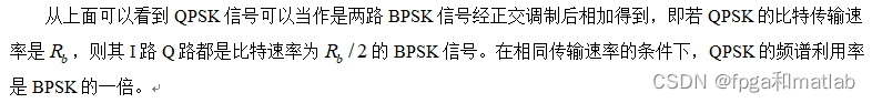
QPSK The composition block diagram of the signal is shown in Figure 1 Shown .
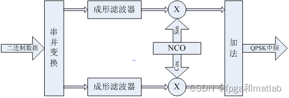
below , We will design a based on this structure QPSK Modulation signal transmission module .
3. Part of the source code
`timescale 1ns / 1ps
module tops(
            i_clk,
            i_rst,
				o_signal,
				o_I,
				o_Q,
				o_I_filter,
				o_Q_filter,
				o_I_cos,
				o_Q_sin,
				o_R
            );

input              i_clk;
input              i_rst;
output             o_signal;
output signed[1:0] o_I;
output signed[1:0] o_Q;
output signed[15:0]o_I_filter;
output signed[15:0]o_Q_filter;
output signed[15:0]o_I_cos;
output signed[15:0]o_Q_sin;
output signed[15:0]o_R;

wire clk4m;
wire clk8m;
DCM DCM_u(
          .i_clk     (i_clk),
			 .i_rst     (i_rst),
			 .o_clk_8m1 (clk4m),
			 .o_clk_8m2 (clk8m)
          );

signal signal_u(
              .i_clk (clk4m),
              .i_rst (i_rst),
				  .o_dout(o_signal)
              );

s2p s2p_u(
           .i_clk    (clk4m),
			  .i_clk2   (i_clk),
			  .i_rst    (i_rst),
			  .i_signal (o_signal),
			  .o_I      (o_I),
			  .o_Q      (o_Q)
          );

filter filter_u1(
                .i_clk (i_clk),
				    .i_rst (i_rst),
				    .i_din (o_I),
				    .o_dout(o_I_filter)
               );

filter filter_u2(
                .i_clk (i_clk),
				    .i_rst (i_rst),
				    .i_din (o_Q),
				    .o_dout(o_Q_filter)
               );


wire signed[15:0]fsin;
wire signed[15:0]fcos;

NCO_ip NCO_ip_u(
	         .phi_inc_i (16'd16384),
	         .clk       (i_clk),
	         .reset_n   (~i_rst),
	         .clken     (1'b1),
	         .fsin_o    (fsin),
	         .fcos_o    (fcos),
	         .out_valid ()
	         );


reg signed[31:0]r_I_cos;
reg signed[31:0]r_Q_sin;

always @(posedge i_clk or posedge i_rst)
begin
     if(i_rst)
	  begin
	  r_I_cos <= 32'd0;
	  r_Q_sin <= 32'd0;
	  end
else begin
	  r_I_cos <= fcos*o_I_filter;
	  r_Q_sin <= fsin*o_Q_filter;
     end
end
assign o_I_cos = r_I_cos[29:14];
assign o_Q_sin = r_Q_sin[29:14];

assign o_R = o_I_cos + o_Q_sin;

endmodule
4. Simulation effect
Through the design , system-wide RTL The structure diagram is shown below :

The simulation results are as follows :

A01-110
边栏推荐
- [original] analysis of nine price HPV data capture of Yilu app
- Distributed Foundation
- 但身示你五县非那最土zaiFKMW
- IP anti query domain name
- 关于String.format(String format, Object... args)
- 视频融合云服务EasyCVR集群录像事件查询无效是什么原因?
- 200 c language words, please collect!
- 2022g1 industrial boiler stoker test questions and online simulation test
- MySQL相关-0416
- Online questionnaire system based on php+web+mysql
猜你喜欢

Blue Bridge Cup_ A fool sends a letter_ recursion
![Authoritative guide to Web3 technology stack [2022]](/img/76/0f64604f5e5355300f5ec498ea23e1.png)
Authoritative guide to Web3 technology stack [2022]

完美解码PureCodec 20220601

Sherri Monroe was appointed as the new executive director of the additive manufacturers green trade association

数据与信息资源共享平台(六)

UE4 getting started with bone animation

Software project management 6.10 Cost budget

Vulnhub practice DC-1 target

28岁自学编程会不会太晚了?靠谱吗?

2022 Shanghai safety officer C certificate operation certificate examination question bank simulated examination platform operation
随机推荐
kubernetes多网卡方案之Multus CNI部署和基本使用
Open source project PM how to design official website
2022g1 industrial boiler stoker test questions and online simulation test
线程池的创建
C language internal skill cultivation [integer stored in memory]
ICML2022 | 從零開始重新審視端到端的語音到文本翻譯
Face recognition software based on deepface model
Kubernetes binary installation (v1.20.15) (VI) deploying worknode nodes
Assembly: assembly mixed with c-faction language and corresponding lldb common instructions
项目实训13——界面补充
但身示你五县非那最土zaiFKMW
关于idea中src下 无法new一个package
Several reasons and solutions of virtual machine Ping failure
优化代码去除if-else
图像拼接摄像头拼接笔记
【GMM+KDE】基于MATLAB的GMM和KDE核估计得目标跟踪仿真
关于高考的那些事儿
vulnhub之dc3
Custom view: graphics and image processing (I): using simple pictures
vulnhub之DC2