当前位置:网站首页>ADS simulation design of class AB RF power amplifier
ADS simulation design of class AB RF power amplifier
2022-07-03 09:57:00 【Running cicada】
ADS Simulation design AB Class RF power amplifier
Power amplifier parameters :
1) Working frequency :2110MHz
2) gain :26dB
3) efficiency :58%
4) Maximum output :36dBm(4W)
5) Third order crossover :-34dBc
6) Leakage pressure :28V
7) Grid voltage :2.1V
Simulation content
1) DC simulation
2) Stability simulation
3) Load traction
4) Source traction
5) Input matching network and output matching network design
6) Schematic simulation
7) Harmonic balance simulation
Specific simulation steps
1. DC simulation
The schematic diagram of DC scanning is as follows :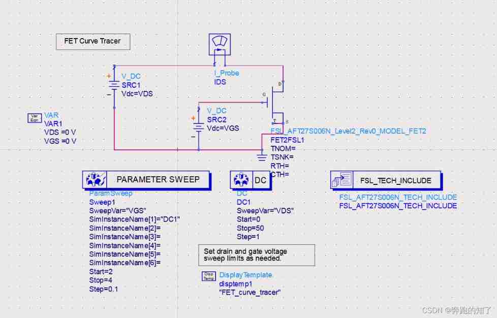
Select static work point 
Here, the bias selects the leakage pressure 28V, Grid voltage 2,1V, Static circuit 184mA Design ;
2. Stability analysis

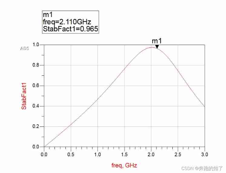
Explain RFin The function of series resistance and parallel resistance :
You can see ,× When the resistance device is dropped , The system is in 2110MHz The stability coefficient at is less than 1;
Here, series resistance and parallel resistance are grounded mainly to improve stability , Make the stability coefficient greater than 1;
1) Series resistance can improve high frequency stability 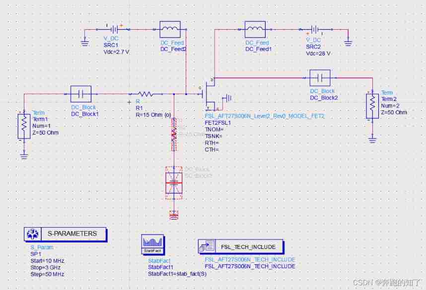
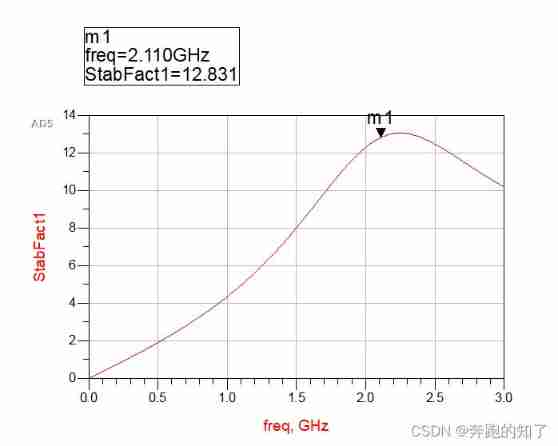
2) The parallel resistance can improve the low-frequency stability 
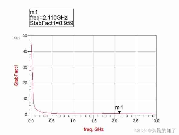
Here we see that the stability at low frequency is greater than 1 requirement
3. Load traction
Insert Load-pull Templates , Replace the power tube in the template with the designed power tube for load traction
Set the parameters 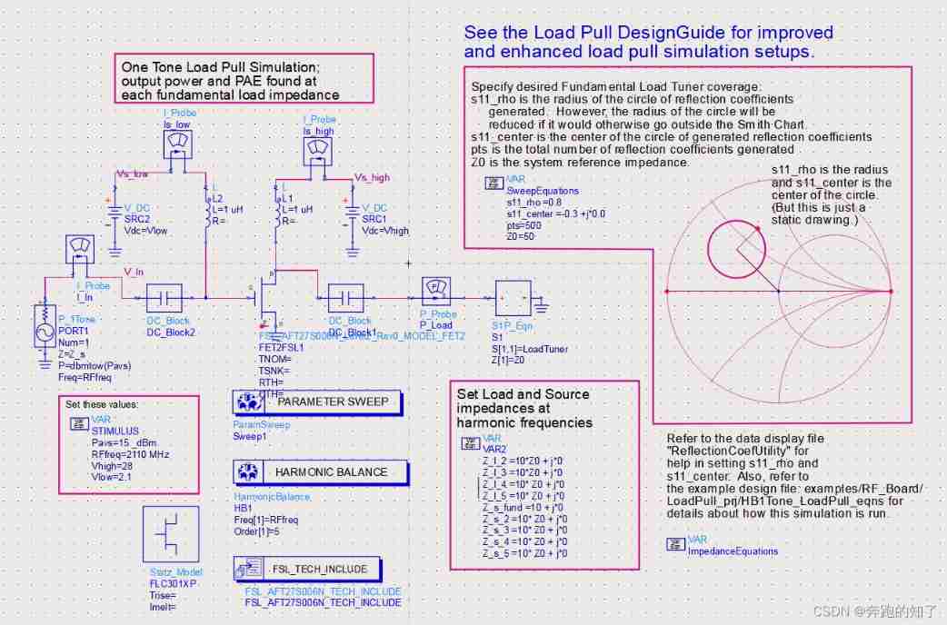

Then select the appropriate load impedance
4. Source traction
Insert source traction template , Replace the power tube and set the parameters 

ditto , Select the appropriate source impedance to design the matching network ;
5. Input matching network design

Insert two term, Set the conjugate impedance of the complex impedance obtained by the front source traction , Design the input matching network 
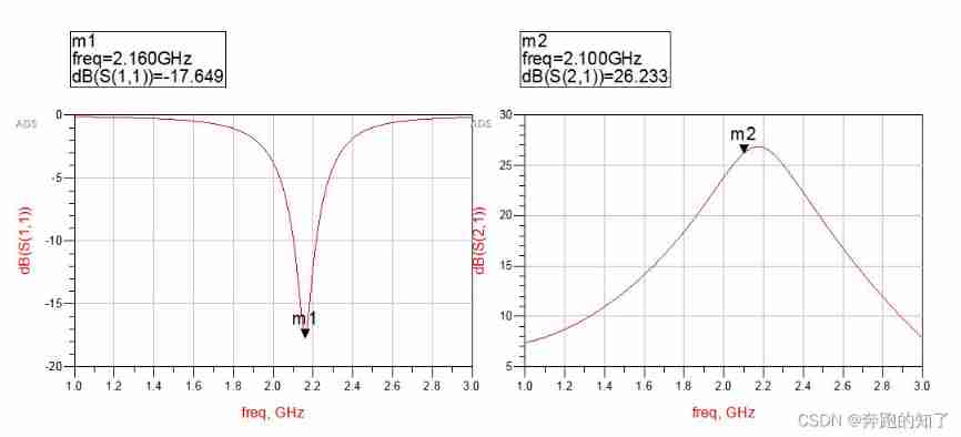
Use Smith Chart The tool gets the input matching network
open S Parameter emulation control , Design the input matching network S Parameter simulation 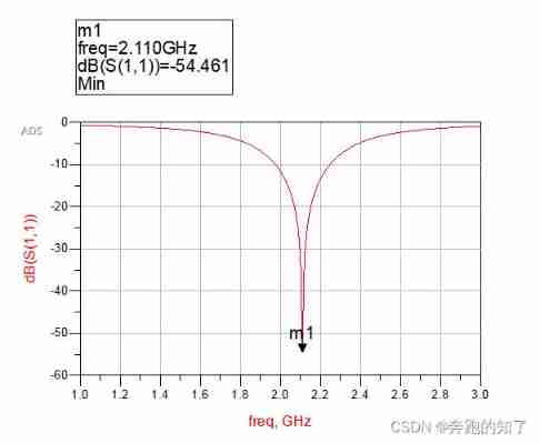
You can see in the 2110MHz It's about ,S11 Yes -54dB
6. Output matching network design
No more details here , Similar to the input matching network design 


7. Schematic simulation
Place the input and output matching networks into the schematic , Add bias circuit and set S Parameter emulation control 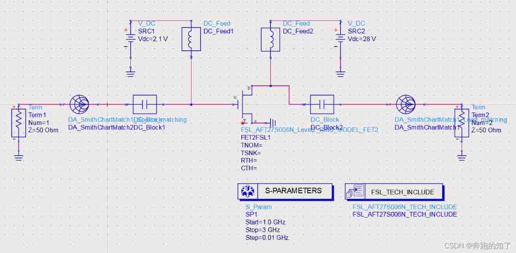
Get in 2110MHz Situated S11 and S21 curve
8. Harmonic balance simulation
First, manually place the following components , Conduct harmonic simulation , The simulation results are as follows 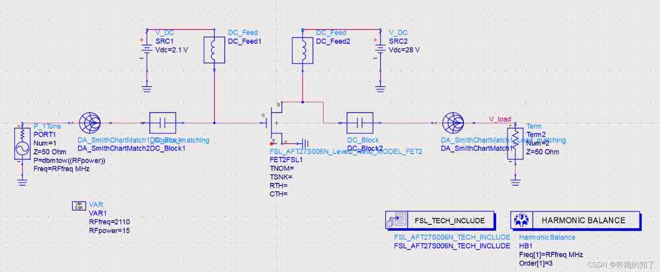
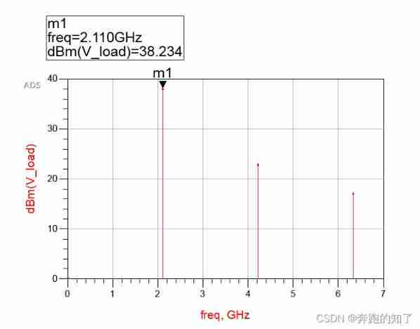
Then put the above schematic diagram Term、 The earth 、 Power Supply × fall , Delete harmonic simulation control , Insert port , Generate Symbol Model 
Finally, insert the harmonic balance simulation template , Conduct harmonic balance simulation 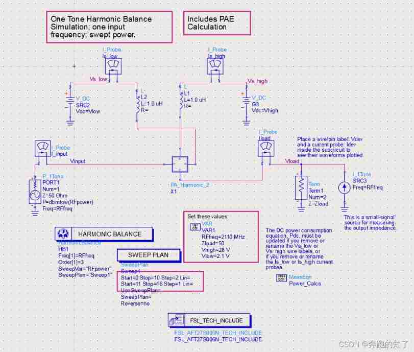
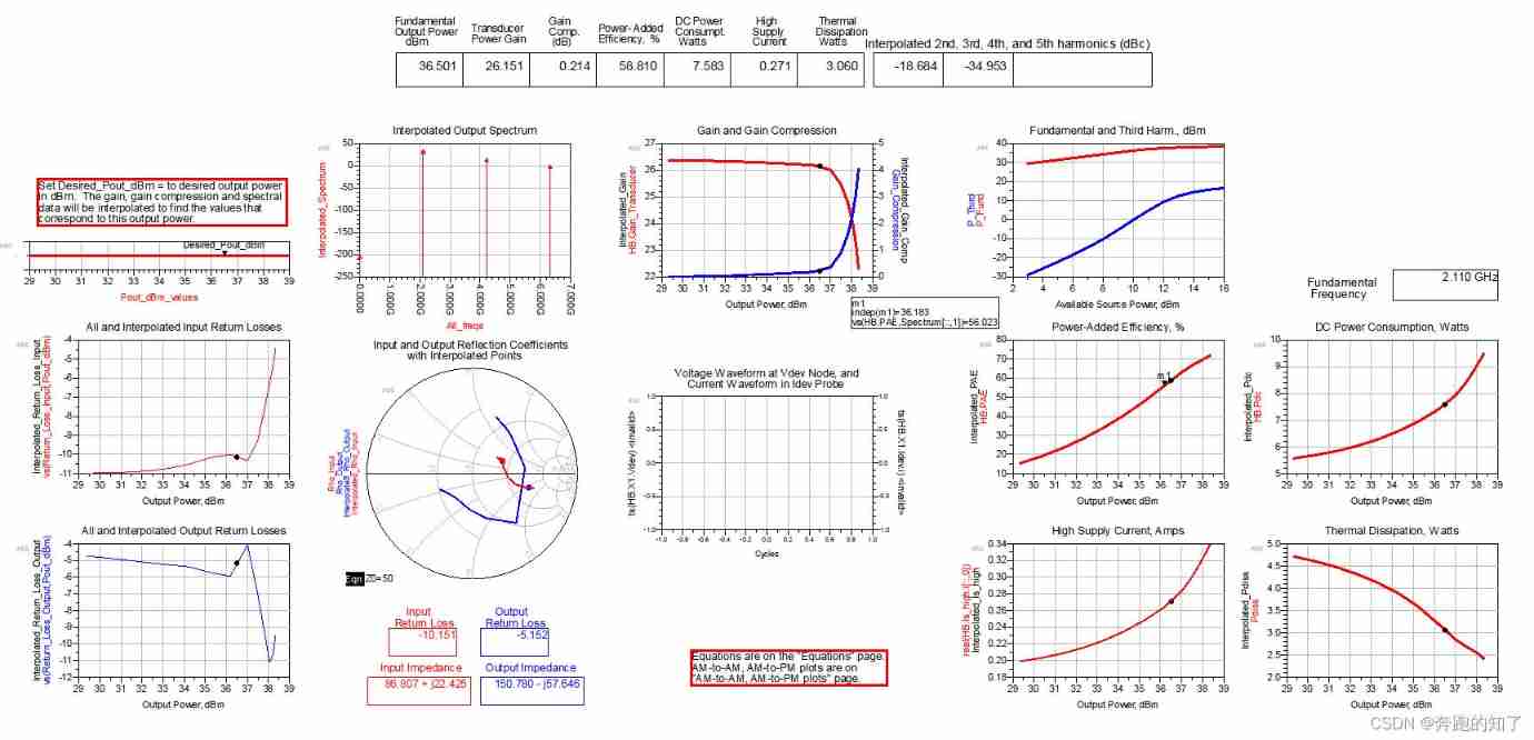
The simulation results are shown in the figure ;
If there are shortcomings , I hope you can correct me .
attach ADS Simulation document
边栏推荐
- Runtime.getRuntime().gc() 和 Runtime.getRuntime().runFinalization() 的区别
- IDEA远程断点调试jar包项目
- STM32 general timer output PWM control steering gear
- 单片机职业发展:能做下去的都成牛人了,熬不动就辞职或者改行了
- MySQL的简单使用(增删改查)
- 学习开发没有捷径,也几乎不存在带路会学的快一些的情况
- Introduction to chromium embedded framework (CEF)
- 端午节快乐!—— canvas写的粽子~~~~~
- STM32 serial communication principle
- A lottery like scissors, stone and cloth (C language)
猜你喜欢
对于新入行的同学,如果你完全没有接触单片机,建议51单片机入门
单片机职业发展:能做下去的都成牛人了,熬不动就辞职或者改行了
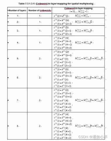
Code word in NR

Education is a pass and ticket. With it, you can step into a higher-level environment
![【顺利毕业】[1]-游览 [学生管理信息系统]](/img/91/72cdea3eb3f61315595330d2c9016d.png)
【顺利毕业】[1]-游览 [学生管理信息系统]

没有多少人能够最终把自己的兴趣带到大学毕业上

Happy Dragon Boat Festival—— Zongzi written by canvas~~~~~
The third paper of information system project manager in soft examination

I didn't think so much when I was in the field of single chip microcomputer. I just wanted to earn money to support myself first
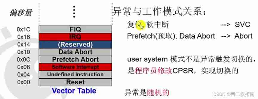
Exception handling of arm
随机推荐
学习开发没有捷径,也几乎不存在带路会学的快一些的情况
在三线城市、在县城,很难毕业就拿到10K
Gpiof6, 7, 8 configuration
All processes of top ten management in project management
2021-01-03
Fundamentals of Electronic Technology (III)__ Fundamentals of circuit analysis__ Basic amplifier operating principle
Intelligent home design and development
应用最广泛的8位单片机当然也是初学者们最容易上手学习的单片机
Stm32f407 key interrupt
Assignment to '*' form incompatible pointer type 'linkstack' {aka '*'} problem solving
Idea remote breakpoint debugging jar package project
2020-08-23
Interruption system of 51 single chip microcomputer
In third tier cities and counties, it is difficult to get 10K after graduation
Synchronization control between tasks
学历是一张通行证,门票,你有了它,可以踏入更高层次的环境里
[CSDN] C1 training problem analysis_ Part IV_ Advanced web
Raspberry pie installation SciPy
UCI and data multiplexing are transmitted on Pusch (Part VI) -- LDPC coding
要选择那种语言为单片机编写程序呢