当前位置:网站首页>Geek DIY open source solution sharing - digital amplitude frequency equalization power amplifier design (practical embedded electronic design works, comprehensive practice of software and hardware)
Geek DIY open source solution sharing - digital amplitude frequency equalization power amplifier design (practical embedded electronic design works, comprehensive practice of software and hardware)
2022-07-02 00:46:00 【Winter_ world】
【 Series column 】: Blogger's output combined with work practice , Column on solving practical problems , Friends, look !
《QT Developing actual combat 》
《 Embedded general development practice 》
《 from 0 To 1 Learn Embedded Linux Development 》
Bring more cases and technical articles to share for a long time ;
Welcome to business project consultation ,10 year + Soft and hard internal skill of the whole stack , Help solve your noble needs .
——————————————————————————————————
Catalog
1 Scheme design and demonstration
1.1 Preamplifier circuit design
1.2 Digital amplitude frequency equalization scheme
1.3 Design scheme of power amplifier circuit
2.3 Digital amplitude frequency equalization
2.3.1 A/D Sampling circuit design
2.3.2 Design of digital amplitude frequency equalization module
2.4 Low frequency power amplifier
4.1 Measurement of preamplifier circuit
4.2 Measurement of band stop network
4.3 Measurement of power amplifier circuit
0 introduction
A digital amplitude frequency equalization power amplifier made a long time ago , Remember, it seems to be the subject of a video game , There are many hardware parts in this design , It was designed many years ago , Read the report made at that time , It's still a little rough , Now share this report , There is a need to do similar design for reference .
The specific content of the original topic can't be found , Now sort out the original report and share it with you , It's also good to be an electronic design reference . This design is based on FPGA Chip based digital amplitude frequency power amplifier , It is pre amplified 、 Band stop network 、 Digital amplitude frequency equalization and low-frequency power amplification circuit are composed of four modules , The analog signal is pre amplified 、 After band stop network , Digital amplitude frequency equalization is realized by digital bandpass filter after analog-to-digital conversion , Then from DA After conversion, it is amplified by the low-frequency power amplifier .
1 Scheme design and demonstration
This system mainly consists of preamplifier 、 Band stop network 、 Digital amplitude frequency equalization and low-frequency power amplification circuit , Its composition block diagram is shown below .

1.1 Preamplifier circuit design
Scheme 1 : Use discrete components to build amplification circuit , It can also meet the design requirements , But the circuit is too complicated , The calculation of magnification is also relatively troublesome .
Option two : utilize NE5532 Complete pre amplification ,NE5532 Output drive capability 600Ω, Input noise voltage 5nV/√Hz , The AC voltage gain conforms to the design conversion rate :9V/μs, Two stage amplification is used to achieve 400 I'm asking for it , After measurement, it meets -1dB The passband is 20Hz~20kHz The requirements of . The circuit design is relatively simple , Easy to calculate . Chips are also relatively cheap .
Options : According to the requirements of the topic and the ease and accuracy of implementation , We choose option two .
1.2 Digital amplitude frequency equalization scheme
Scheme 1 : Measure the amplitude frequency characteristics of the band stop network , utilize multism The design tool obtains the coefficients of the bandpass filter , use FPGA Inside IP CORE Nuclear FIR The filter module realizes bandpass FIR Digital filter , Thus, the signal is compensated .
Option two : utilize AD Sample the output waveform of the band stop network , Convert analog signals into digital signals and store , Then through the fast Fourier transform FFT Convert it into frequency domain signal , With 10KHz The amplitude of the frequency is the reference and compared with the amplitude of its remaining frequency points , Frequency compensation , Then inverse fast Fourier transform is performed for each frequency point IFFT After by DA Output .
Options : The advantage of scheme 1 is that the amount of data calculation is small , The disadvantage is that the band-pass filter is difficult to fully compensate the attenuation of the band stop filter . The advantage of scheme 2 is that it can compensate for the full frequency band , The disadvantage is the large amount of data storage and calculation , According to enforceability , We choose option one .
1.3 Design scheme of power amplifier circuit
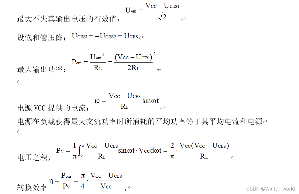
Scheme 1 : Class a amplifier , It can be operated by single tube or push-pull , The advantage of class a amplifier is no crossover distortion and switching distortion , Theoretical efficiency 50%.
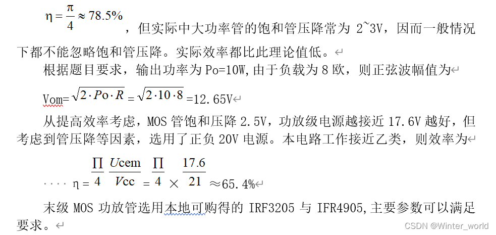
Option two : Adopt class B amplification circuit , Low pipe consumption , The quiescent current is zero , The advantage is higher efficiency , The theoretical efficiency is 78.5%, The disadvantage is that the push-pull power amplifier tube works in the nonlinear region , There is crossover distortion .
Option three : Adopt class A and class B push-pull power amplifier . The previous level is NE5532 Put a lot of for the core composition, about 3.5 Times the pre amplification circuit , The next stage is composed of NMOS Management and PMOS Tubes form complementary push-pull outputs , By adjusting the potentiometer R7 and R8 Provide a suitable bias voltage for the transistor , To avoid crossover distortion . in addition , Due to the high power of the power amplifier , We use heat sinks to dissipate heat and protect transistors .
Options : According to the title requirements , Take into account the efficiency of power amplifier and output power , And passband requirements , We choose option three .
2 Circuit and programming
According to the task required by the topic , The digital amplitude frequency equalization power amplifier includes preamplifier 、 Band stop network 、 Digital amplitude frequency equalization and low frequency power amplification , Because the four modules are relatively independent , The following is the principle analysis and circuit design .
2.1 Preamplifier
The preamplifier is mainly used to amplify the voltage of small signals , Its distortion and noise have the greatest impact on the system , It is an indicator that should be given priority . This amplification circuit adopts chip NE5532.
First stage magnification : Voltage follower R7
Second stage magnification : Adjust the potentiometer R9, The magnification of the two stages is 500 times .
The total magnification is 500 times , Meet the requirements of the topic . Because the output resistance of the amplifier circuit composed of operational amplifier is very small , Close to the 0 ohm , So connect the amplifier output in series R14, Make the output resistance 600 o .

2.2 Band stop network
The design stopband network is shown in the figure below :

Simulation results :
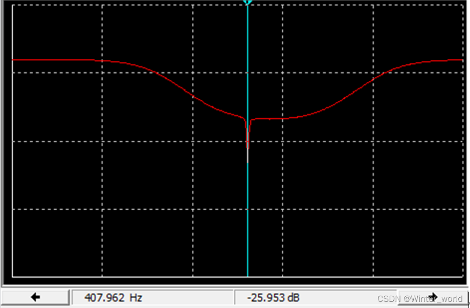
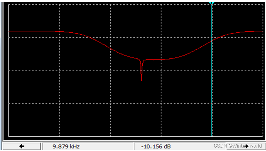
From the simulation results :
f=407.962kHz when , The attenuation is 25.953Db;f=9.879kHz when , The attenuation is 10.156Db, Meet the requirements .
2.3 Digital amplitude frequency equalization
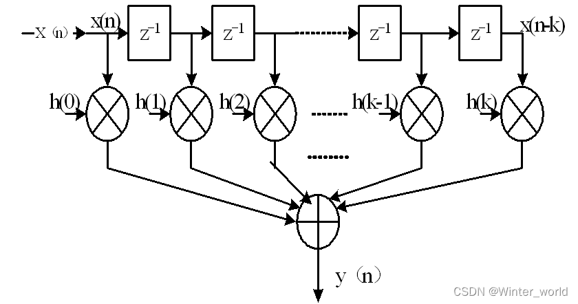
For the digital equalizer of this design FIR Digital filter , In order to compensate , According to the transfer function of the band stop network H(s) Use DSP Builder Design a transfer function opposite to that of the band stop network 200 Step FIR Bandpass filter .
Its system function can be recorded as :
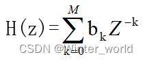
among M yes FIR Number of zeros of filter , That is, the order of delay . Its output sequence satisfies the following equation :
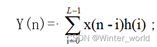
among x(n) Input sampling sequence ,h(i) It's the filter coefficient ,L Is the coefficient length of the filter ,y(n) Represents the output sequence of the filter . The filter structure is shown in the figure 4 Shown :
2.3.1 A/D Sampling circuit design
According to the index of the subject and the requirements of system frequency , We choose AD574 chip design A/D Sampling circuit , use 8 Bit bipolar voltage input mode , The input voltage range is -5V to +5V, Its sampling frequency can reach 30KHZ, The sampling circuit design is shown in the figure below .

2.3.2 Design of digital amplitude frequency equalization module
The schematic diagram of digital amplitude frequency equalization module is shown in the figure below .

If we want to realize the complete compensation of band stop network , that FIR The filter and the band stop network shall be mutually inverse systems , use MATLAB The software designs FIR After the unit impulse response that the filter should have, the filter coefficient is imported into QUARTUS ii Generated inside FIR Of IP CORE, utilize FPGA The core board connects the periphery AD And DA The circuit realizes the function of digital amplitude frequency equalization .
According to the requirements of this topic , We design FIR The signal processing range of the filter is 20Hz~10KHz, The order of the filter is 200 rank , The sampling frequency of the system is 30KHz, The software block diagram of the system is shown in the figure below .

2.3.3 D/A Design of conversion circuit
According to the topic, I want to go , We chose DAC0832 As an analog-to-digital conversion chip .DAC0832 yes 8bit Of DA device , The circuit of this part is shown in the figure below .

2.4 Low frequency power amplifier
Design of power amplifier circuit Main task yes , Within the allowable distortion limit , Provide enough power to the load as efficiently as possible . The basic requirements of power amplifier circuit are :
The output power should be large , Output power PO= UO ×IO , To obtain large output power , Not only high output voltage is required , And the output current is required to be large . So consider MOS Limit parameters of tubes , Be careful MOS Tube safety . Be efficient , The process of amplifying the signal is MOS The tube changes according to the input signal , The process of converting the energy provided by DC power supply into AC energy , Its conversion efficiency is the ratio of the signal power obtained on the load to the power supplied by the power supply .
The power amplifier level circuit is mainly composed of NE5532 And two pairs of high power at the last power stage MOS Tube composition , As shown in the figure below :

Ideally, the pressure drop in the saturated pipe is not considered ,
3 Software design and process

4 The system test
Test instruments : Digital signal generator SFG-1013, Digital storage oscilloscope GDS-1102, DC power supply 1731SLL3A.
4.1 Measurement of preamplifier circuit
a. Magnification test conditions : Input AC signal , The frequency is 1KHz, Valid values are 5mV, Input amplitude 7.1mV.
Magnification test results : Output peak to peak 7.12V , Zoom in approx 500 times .
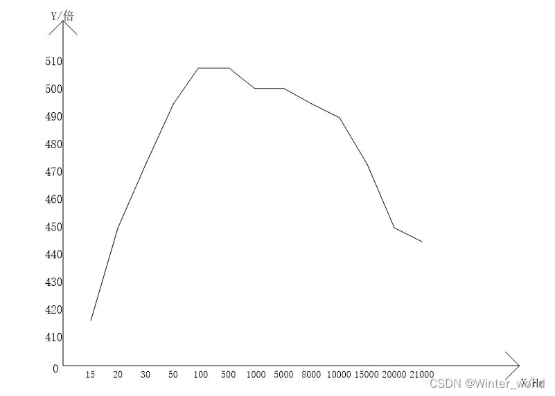
b.-1dB Passband test conditions : Input AC signal , Valid values are 5mV, Input amplitude 7.1mV , The frequency is 20Hz-20kHz.
-1dB Passband test conditions test results :
Input signal frequency (Hz) | Input voltage peak to peak (mv) | Peak to peak output voltage (V) | Magnification |
15 | 14.2 | 5.92 | 416.9 |
20 | 14.2 | 6.40 | 450.7 |
30 | 14.2 | 6.72 | 473.2 |
50 | 14.2 | 7.04 | 495.8 |
100 | 14.2 | 7.20 | 507.0 |
500 | 14.2 | 7.20 | 507.0 |
1000 | 14.2 | 7.12 | 501.4 |
5000 | 14.2 | 7.12 | 501.4 |
8000 | 14.2 | 7.04 | 495.8 |
10000 | 14.2 | 6.88 | 484.5 |
15000 | 14.2 | 6.72 | 473.2 |
20000 | 14.2 | 6.40 | 450.7 |
21000 | 14.2 | 6.32 | 445.1 |
From the above test data ,-1dB The passband is 20Hz-20kHz.
c. The output resistance is 600Ω.
4.2 Measurement of band stop network
Testing conditions : Input AC signal , Valid values are 5mV, Input amplitude 7.1mV , The frequency is 20Hz-20kHz.
test result :
frequency (Hz) | 20 | 100 | 300 | 500 | 800 | 1k | 1.5 | 1.9 |
Output voltage peak peak (v) | 5.04 | 2.04 | 1.06 | 0.94 | 0.90 | 0.90 | 0.94 | 1.00 |
2k | 2.1k | 2.5k | 3k | 4K | 6k | 10k | 15k | 20k |
1.06 | 1.06 | 1.14 | 1.26 | 1.52 | 2.04 | 2.96 | 3.84 | 4.32 |
From the above test results ,f=800Hz when ,V=0.90v, f=10kHz when ,V=2.96v.
With 10k Benchmarking ,800Hz Attenuation at 10.34dB, It is more than or equal to 10dB The requirements of .
4.3 Measurement of power amplifier circuit
Testing conditions : Input AC signal , Valid values are 5mV, Input amplitude 7.1mV , The frequency is 1kHz.
test result :
a. stay 8W Output voltage measured on load Vo =11.103v Calculated output power P1=15.41w
Use an oscilloscope to observe the output voltage waveform without distortion .
b. DC supply voltage =20v, Over DC power supply current =0.62A, Calculated DC power supply P2=24.8w, Then efficiency =62.14%.
The appended drawings : Front circuit data line chart
5 summary
This design impression should be that the blogger didn't go home in the summer when he was in College , Preparing for the national competition is also a practice topic for the provincial competition , This design is shared here for the reference of friends in related fields . At that time, I was impressed by MOS Many tubes were burnt out , Only then did I know how important it is to add heat sinks to high-power things . Electronic design may be confused at the beginning , Many people think that analog electricity is a very metaphysical thing , Listening to others say something difficult makes me afraid , Here is a piece of advice for beginners : Dare to try new things , Have your own judgment before you act ,Keep hungry, keep foolish.
As in the 202206301650, Filed
———————————————————————————————————
This article is an original blog article , No reprint without the permission of the blogger !
If this article is helpful to you , Lift your little hand to make a fortune , Focus on / Comment on / give the thumbs-up / Collection , Is the greatest support for me !
I wish you a promotion and a raise , have a bright future !
边栏推荐
- Take the enclave Park as a sample to see how Yuhua and Shaoshan play the song of Chang Zhu Tan integrated development
- [JS download files through url]
- How to improve data quality
- 2022 safety officer-a certificate examination questions and online simulation examination
- EMC circuit protection device for surge and impulse current protection
- Schrodinger's Japanese learning applet source code
- Comprehensive usage and case questions of sub query of SQL data analysis [patient sorting]
- JS——图片转base码 、base转File对象
- [CTF] bjdctf 2020 Bar _ Bacystack2
- [bottom pop-up selector] uniapp picker component - scroll selector popped up at the bottom
猜你喜欢

Friends circle community program source code sharing

Source code of Qiwei automatic card issuing system

2022 safety officer-b certificate examination practice questions simulated examination platform operation
Some understandings of graph convolution neural network r-gcn considering relations and some explanations of DGL official code
SQL Server 安裝指南
Bc35 & bc95 onenet mqtt (old)
gradle
EMC circuit protection device for surge and impulse current protection
【八大排序④】归并排序、不基于比较的排序(计数排序、基数排序、桶排序)
使用 ES 实现疫情地图或者外卖点餐功能(含代码及数据)
随机推荐
cookie、session、tooken
Is it safe and reliable to open an account in Caixue school and make new debts?
Window sorting functions rank and deny for SQL data analysis_ rank、raw_ Number and lag, lead window offset function [usage sorting]
Xinniuniu blind box wechat applet source code_ Support flow realization, with complete material pictures
Kyushu cloud and Intel jointly released the smart campus private cloud framework, enabling new infrastructure for education
Practical calculation of the whole process of operational amplifier hysteresis comparator
Friends circle community program source code sharing
Is it safe to buy funds in a securities account? Where can I buy funds
Ldr6035 smart Bluetooth audio can continuously charge and discharge mobile devices
AIX存储管理之卷组的创建(一)
[leetcode] number of maximum consecutive ones
BiLSTM-CRF代码实现
Node——Egg 创建本地文件访问接口
Node——生成微信权限验证配置
Halcon knowledge: an attempt of 3D reconstruction
RFID让固定资产盘点更快更准
程序员该如何更好的规划自己的职业发展?
Node - generate wechat permission verification configuration
Node -- egg implements the interface of uploading files
How to improve data quality