当前位置:网站首页>Digital signal processing-07-dds IP application example
Digital signal processing-07-dds IP application example
2022-06-21 06:07:00 【Vuko-wxh】
Preface
This article is based on DDS Build simulation engineering , Including single channel project 、 Multi channel project 、 Use DDS Perform mixing operation .
single channel IP To configure
Build a new blank project ,FPGA Any model , add to DDS IP To the project , Double click to open the configuration item interface . This interface can be configured DDS Related configuration options and basic parameters of . Here we will focus on the commonly configured parameters .
The system clock : by DDS Working system clock .
Number of channels : Select the number of channels according to the design requirements .
Spurious free dynamic range (SFDR): Input the corresponding value here to calculate the output DDS The bit width of the data ,N representative DDS The number of output bits . The following formula can be used to 45 Make a conversion , After calculation N=7.47, The output bit width obtained by rounding up is 8.
S F D R = 20 ∗ l o g ( 2 N ) SFDR = 20*log(2^N) SFDR=20∗log(2N)Frequency resolution : Frequency resolution is used to control the minimum resolution accuracy .

After configuration, configure the basic information on the next page , Basically keep the default , Here I just want to check the waveform , So the phase output is turned off .

The configuration on the third page can be left as default .

Page 4 output frequency configuration , Set the output here 10M

You can also see the relevant information of the output signal in the summary , Here we can briefly calculate phase width Of 28Bits How did you get here . The parameters and DDS The operating frequency of the and the enabling channel , And frequency resolution . By the following formula , The current setting can be obtained by deformation Frequency Resolution.DDS The clock is 100MHz, Passageway is 1, Phase width 28Bits, The converted frequency resolution is 0.37252902984619140625. Take the whole number up , Get the currently set 0.4Hz The resolution of the . Given the frequency resolution, the bit width can also be converted , However, the bit width obtained at this time is 2 To the power of .
2 P h a s e W i d t h = D D S c l o c k C h a n n e l s × F r e q u e n c y R e s o l u t i o n 2^{Phase\,Width} =\frac {DDS\,clock}{Channels × Frequency \, Resolution} 2PhaseWidth=Channels×FrequencyResolutionDDSclock
At the same time, the vector increment can be calculated according to the previous related parameters . The value of the increment can be calculated from the parameters brought in .
P h a s e I n c r e m e n t = 2 P h a s e W i d t h × o u t f r e q u e n c y D D S c l o c k Phase Increment = \frac {2^{Phase\,Width} × out\,frequency}{DDS\,clock} PhaseIncrement=DDSclock2PhaseWidth×outfrequency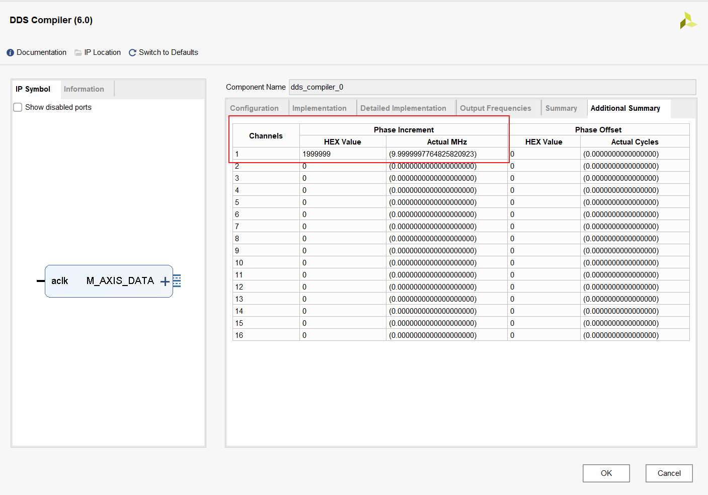
Single channel instance
Top level call
According to the above IP After the configuration is completed, it will be configured in top Layer , Then the single channel can be completed DDS Call use of . The top-level module calling code is as follows :
module top(
    input clk
    );

    wire m_axis_data_tvalid_ch1;
    wire [7:0] m_axis_data_tdata_ch1;
    // Single channel test
    dds_compiler_0 ch1_dds(
    .aclk(clk),                              // input wire aclk
    .m_axis_data_tvalid(m_axis_data_tvalid_ch1),  // output wire m_axis_data_tvalid
    .m_axis_data_tdata(m_axis_data_tdata_ch1)    // output wire [7 : 0] m_axis_data_tdata
    );
endmodule
Write simulation
To write testbench, Because the top layer only gives a clock input port , So we only need to simulate the clock , single channel DDS Test the following :
`timescale 1ns / 1ps
module tb_top;

// top Parameters
parameter PERIOD  = 10;

// top Inputs
reg   clk                                  = 0 ;

// top Outputs

initial
begin
    forever #(PERIOD/2)  clk=~clk;
end

top  u_top (
    .clk(clk)
);

initial
begin
 	#10000;
    $finish;
end

endmodule
After writing, you can directly click Run simulation test .
test result
Run the simulation to check the waveform results , Add the waveform of the top instantiation module to the waveform window , You can get the value displayed in hexadecimal in digital mode , The value can be converted into waveform display for easy observation .

Set the hexadecimal format and display mode of the data , Here, modify the channel data to analog Pattern , Base is changed to signed decimal .


Add cursor after modification , It can be observed that the period of the output waveform is 100ns, That is to say 10MHz, The output waveform frequency is consistent with the setting .

Multi channel instance
Reopen IP Configure the interface or create a new one DDS IP, Change the number of channels , I'm going to set it to 3. Enable phase output signal , Check the phase change . because DDS Of IP The core multichannel is time-sharing multiplexed , Therefore, it is better to enable the channel in the detail implementation configuration interface ID For normal output of single channel signal waveform . The rest can remain the default .

Configure the output frequency as 10MHz、3MHz、4MHz.

Configuration complete click OK, Instantiate the module .
Top level call
The top-level module calling code is as follows :
module top(
    input clk
    );

    wire m_axis_data_tvalid_ch1;
    wire [7:0] m_axis_data_tdata_ch1;

    wire          m_axis_data_tvalid_ch3;
    wire [7 : 0]  m_axis_data_tdata_ch3;
    wire [1 : 0]  m_axis_data_tuser_ch3;
    wire          m_axis_phase_tvalid_ch3;
    wire [31 : 0] m_axis_phase_tdata_ch3;
    wire [1 : 0]  m_axis_phase_tuser_ch3;

    // Multichannel test
    dds_compiler_1 multi_ch_dds(
    .aclk(clk),                                // input wire aclk
    .m_axis_data_tvalid(m_axis_data_tvalid_ch3),    // output wire m_axis_data_tvalid
    .m_axis_data_tdata(m_axis_data_tdata_ch3),      // output wire [7 : 0] m_axis_data_tdata
    .m_axis_data_tuser(m_axis_data_tuser_ch3),      // output wire [1 : 0] m_axis_data_tuser
    .m_axis_phase_tvalid(m_axis_phase_tvalid_ch3),  // output wire m_axis_phase_tvalid
    .m_axis_phase_tdata(m_axis_phase_tdata_ch3),    // output wire [31 : 0] m_axis_phase_tdata
    .m_axis_phase_tuser(m_axis_phase_tuser_ch3)    // output wire [1 : 0] m_axis_phase_tuser
    );
The simulation test
The simulation file can keep the single channel test unchanged , Click Run behavior level simulation , Add the signal waveform to observe the following . The data is not a sinusoidal waveform obtained directly , It's a mess .

Zoom in tuser The signal can be observed , Data and phase channels tuser The signal is periodic , there tuser Signals represent IP Set in the chen ID, So it is time-sharing multiplex output 3 The signals of two channels should be sorted by writing simple logic .

Top level module modification
According to the tuser One step deposit of output data for judging conditions , Thus, the waveform data of three channels can be obtained . The code is as follows :
module top(
    input clk
    );

    // Multichannel test
    dds_compiler_1 multi_ch_dds(
    .aclk(clk),                                // input wire aclk
    .m_axis_data_tvalid(m_axis_data_tvalid_ch3),    // output wire m_axis_data_tvalid
    .m_axis_data_tdata(m_axis_data_tdata_ch3),      // output wire [7 : 0] m_axis_data_tdata
    .m_axis_data_tuser(m_axis_data_tuser_ch3),      // output wire [1 : 0] m_axis_data_tuser
    .m_axis_phase_tvalid(m_axis_phase_tvalid_ch3),  // output wire m_axis_phase_tvalid
    .m_axis_phase_tdata(m_axis_phase_tdata_ch3),    // output wire [31 : 0] m_axis_phase_tdata
    .m_axis_phase_tuser(m_axis_phase_tuser_ch3)    // output wire [1 : 0] m_axis_phase_tuser
    );
    reg [7 : 0] data10MHz;
    reg [7 : 0] data3MHz;
    reg [7 : 0] data4MHz;
    always @(posedge clk) begin
        case(m_axis_data_tuser_ch3)
            0:data10MHz<=m_axis_data_tdata_ch3;
            1:data3MHz<=m_axis_data_tdata_ch3;
            2:data4MHz<=m_axis_data_tdata_ch3;
        endcase
     end
    reg [31 : 0] phase10MHz;
    reg [31 : 0] phase3MHz;
    reg [31 : 0] phase4MHz;
    always @(posedge clk) begin
        case(m_axis_data_tuser_ch3)
            0:phase10MHz<=m_axis_phase_tdata_ch3;
            1:phase3MHz<=m_axis_phase_tdata_ch3;
            2:phase4MHz<=m_axis_phase_tdata_ch3;
        endcase
    end
The waveform is as follows , As you can see from the diagram , After logical sorting , The waveform output of the three channels is normal , Here you can see that compared to single channel output 10MHz The sine wave of the signal , At this time, the output waveform cannot see the period of the sinusoidal waveform from the time domain , The reason is that when multiple channels are enabled , The reference clock of the corresponding channel is the system clock divided by the number of channels , Now... Is set 100MHz Working clock , Can make 3 Channels , So the reference clock of a single channel is 33.333MHz, about 10MHz For the signal , It is equivalent to only three points in a cycle , Therefore, the time domain characteristics cannot be observed normally , But the frequency domain characteristic still exists .

Mixing examples
Mixing principle
It is necessary to move the frequency spectrum of the input if signal , Mixing operation is required , Move the spectrum to high frequency or low frequency , In fact, it is like a car driving on a high-speed road or a low-speed road , High frequency and low frequency are carriers , A carrier of information . In digital signal processing , Moving the spectrum is to combine a local seismic signal with an input signal , Mixing , So you can get a composite signal , Here we look at the composite signal through the formula .

there α and β It refers to two frequency signals , When you multiply each other, you get two frequency signals , One is α + β, The other is α – β. The logo in the above figure is fout The signal should be f1+f2 and f1-f2 Composite signal .
Use the output from the multi-channel instance 3MHz and 4Mhz, Perform mixing operation , obtain 1MHz and 7MHz Mixed signal . Call the multiplier to perform mixing and multiplication .
Top level modules
module top(
    input clk
    );

    wire          m_axis_data_tvalid_ch3;
    wire [7 : 0]  m_axis_data_tdata_ch3;
    wire [1 : 0]  m_axis_data_tuser_ch3;
    wire          m_axis_phase_tvalid_ch3;
    wire [31 : 0] m_axis_phase_tdata_ch3;
    wire [1 : 0]  m_axis_phase_tuser_ch3;

    // Multichannel test
    dds_compiler_1 multi_ch_dds(
    .aclk(clk),                                // input wire aclk
    .m_axis_data_tvalid(m_axis_data_tvalid_ch3),    // output wire m_axis_data_tvalid
    .m_axis_data_tdata(m_axis_data_tdata_ch3),      // output wire [7 : 0] m_axis_data_tdata
    .m_axis_data_tuser(m_axis_data_tuser_ch3),      // output wire [1 : 0] m_axis_data_tuser
    .m_axis_phase_tvalid(m_axis_phase_tvalid_ch3),  // output wire m_axis_phase_tvalid
    .m_axis_phase_tdata(m_axis_phase_tdata_ch3),    // output wire [31 : 0] m_axis_phase_tdata
    .m_axis_phase_tuser(m_axis_phase_tuser_ch3)    // output wire [1 : 0] m_axis_phase_tuser
    );
    reg [7 : 0] data10MHz;
    reg [7 : 0] data3MHz;
    reg [7 : 0] data4MHz;
    always @(posedge clk) begin
        case(m_axis_data_tuser_ch3)
            0:data10MHz<=m_axis_data_tdata_ch3;
            1:data3MHz<=m_axis_data_tdata_ch3;
            2:data4MHz<=m_axis_data_tdata_ch3;
        endcase
     end
    reg [31 : 0] phase10MHz;
    reg [31 : 0] phase3MHz;
    reg [31 : 0] phase4MHz;
    always @(posedge clk) begin
        case(m_axis_data_tuser_ch3)
            0:phase10MHz<=m_axis_phase_tdata_ch3;
            1:phase3MHz<=m_axis_phase_tdata_ch3;
            2:phase4MHz<=m_axis_phase_tdata_ch3;
        endcase
    end
    // Mixing test
    wire [15 : 0]  mixer_singal;
    mult_gen_0 mult_mixer (
        .CLK(clk),  // input wire CLK
        .A(data3MHz),      // input wire [7 : 0] A
        .B(data4MHz),      // input wire [7 : 0] B
        .P(mixer_singal)      // output wire [15 : 0] P
    );
endmodule
The simulation test
The simulation file can keep the single channel test unchanged , Click Run behavior level simulation , Add signal waveform and modify waveform settings , The signal effect after mixing can be obtained .

边栏推荐
- 代码生成器文件运行出错:The server time zone value ‘�й���ʱ��‘ is unrecognized or represents more than one time
- 双调查找:数组先递增后递减
- DosBox安装
- FPGA - 7系列 FPGA SelectIO -05- 逻辑资源之OLOGIC
- Improved Object Categorization and Detection Using Comparative Object Similarity
- Sub-Category Optimization for Multi-View Multi-Pose Object Detection
- 成立时间用了时间插件,但在网页上修改参数的时候,如果未修改时间第一次保存会报错,第二次才行
- 三维引擎软件Vizard入门
- Copy the code generated by the code generator to the idea. How to solve the error reported by the web address after running
- 图片隐写术:方法1
猜你喜欢

Improve the determination of the required items of business details. When the error information is echoed according to the returned status code, the echoed information is inconsistent with the expecta

【JVM】方法区

C语言课程设计(服装管理系统详解)
![[MySQL] SQL statement execution process of MySQL](/img/c8/76726de7ae3521f709e336a60ae3a2.png)
[MySQL] SQL statement execution process of MySQL

Latest analysis on operation of refrigeration and air conditioning equipment in 2022 and examination question bank for operation of refrigeration and air conditioning equipment

You have an error in your SQL syntax; check the manual that corresponds to your MYSQL server

Broadcast mechanism of numpy

397 linked list (206. reverse linked list & 24. exchange nodes in the linked list in pairs & 19. delete the penultimate node of the linked list & interview question 02.07. link list intersection & 142
Laravel

Aurora8B10B IP使用 -01- 简介与端口描述
随机推荐
Sub-Category Optimization for Multi-View Multi-Pose Object Detection
Do you want to manually implement CSDN dark mode for web page '?
二叉排序树的基本操作
应用在洗衣机触摸屏中的触摸芯片
tf.AUTO_REUSE作用
上手自定义线程池
397 linked list (206. reverse linked list & 24. exchange nodes in the linked list in pairs & 19. delete the penultimate node of the linked list & interview question 02.07. link list intersection & 142
tf.QueueBase
构建和保护小型网络考试
Connection refused : no futher information : localhost/127.0.0.1:6379
深度理解RNN的梯度消失和LSTM为什么能解决梯度消失
tf.compat.v1.get_default_graph
应用在LED植物照明中的LED照明灯
kali快捷键和设置方式
Attack and defense world PHP_ rce
数据接口请求异常,you have an error in your SQL syntax;check the manual that corresponds to your MYSQL server
牛客-TOP101-BM25
Dosbox installation
应用在电视触摸屏中的十四通道智能触摸芯片
The usage of Roca data visualization API 2.0 of Gaode map