当前位置:网站首页>HUST network attack and defense practice | 6_ IOT device firmware security experiment | Experiment 2 MPU based IOT device attack mitigation technology
HUST network attack and defense practice | 6_ IOT device firmware security experiment | Experiment 2 MPU based IOT device attack mitigation technology
2022-06-26 11:28:00 【shandianchengzi】
List of articles
- Experiment two be based on MPU Internet of things device attack mitigation technology
Write at the top : Pay attention to downloading the latest version lib(6 month 2 It's a new edition ), And combine your own lib analysis . The analysis process is a little long , To help you find your address 、 And understand it . actually , What needs to be written into the report Only subtasks 2 So a little .
Experiment two is troublesome , Additional content I have actually written into my blog , If you want to write , Please tidy up by yourself . Experiment three is very simple , Experiment 2 is troublesome and long , Considering that you should also write a report , I will separate the first experiment two .
Experiment two be based on MPU Internet of things device attack mitigation technology
The experimental requirements
Experimental lib A number of... Are opened in the library code MPU Regional protection
Please reconfigure according to different subtasks MPU The area is unprotected
- The subtasks 1 Remove the non writable protection of the code segment and change the specified code segment to writable
- The subtasks 2 Unprotect a specific peripheral area and change the specified peripheral area to read / write
notes : please Trigger by reverse analysis Memfault Instructions , Thus, while meeting the task requirements, the most Less MPU Area configuration 、 The smallest MPU Regional scope , The smallest privilege level .
Privilege level sorting :rwx( Readable, writable, and executable )> rw>rx>r> No authority
Be careful : Mission 2 Use architecture mps2-an386.
Experiment preparation
Keil Installation and use
Installation cracking process :
- install
Keil5: All the wayNextJust go , Name and e-mail address can be filled in at will , The installation driver is selected , The installation path should not contain Chinese , Or default directly . - Crack
Keil5: Open the just installed with administrator privilegesKeil5, Close the pop-up window for installing packages , And then clickFile-License Management, CopyCIDTo crack software . Crack software fill inCID、 Set upTargetbyARMafter , Click onGenerateGenerateLIC, Paste theKeil5OfLICIn the input box . Click onAdd LICJust go . - install
ARM CMSDK_CM4_FP: The teacher sent itKeil5The default is not what we wantARM CMSDK_CM4_FP. But the teacher also sent two.packfile , Double click Install . All the wayNext, Installation path and Keil5 The installation directory of corresponds to .
Create a new project and add a file :
Project-New uVersion Project , Then the configuration is directly according to the experimental instruction , Also directly follow the instructions . Add files that you can drag directly into . Compilation is Project-build.
Be careful : If you have installed other versions of
Keil, And created a new project , Remember to delete... From the project directoryListings、Objects、RTE, Otherwise, it will automatically read the configuration from these directories first , The version is wrong .
If the configuration items are completely correct , It is completely consistent with the instructions , When you run directly, you will 0 Error.
The executable file will be generated in Objects/ Next , Run the following command to run :
~/qemu-7.0.0/build/qemu-system-arm -M mps2-an386 -cpu cortex-m4 -m 16M -nographic -d in_asm,nochain -kernel ~/exp6/task2/task2.axf -D log.txt
Analysis gives .c/.h/.lib Content and function of the document
Let's briefly analyze task2.c The content of .
main function :
① Define unsigned integer variables a, The assignment is at the end of the student ID 4 position ;
② call prvSetupHardware(), Hardware initialization ;
③ call xTaskCreate, Create tasks , The task is vTaskStart, The task name is "Task2", The permission is privilege level ;
④ call StartFreeRTOS(a);
⑤ Use for(;;) Let the program not exit .
stay vTaskStart In the task of , Called AttackTest().
After the reverse analysis , It can be further determined that : stay
StartFreeRTOS(a)Contains the start of the task sequence . When it starts Task2 after , Will callAttackTest(). If AttackTest There is no triggerMemMange_Handlerabnormal , Under certain conditions , It will print out smoothlyflag; When AttackTest After triggering an exception , The task will end .
MemMange_HandlerThe exception has a trigger delay , So the old lib Always when an exception has not been triggered , It's already printedflag, So the teacher updated the new version lib file .
By looking at task2.h, You can see AttackTest、prvSetupHardware、StartFreeRTOS Function declaration of , The concrete implementation of these functions , It is in task2x_xx.lib In file .
When the project is built , The contents of all the files will be linked to the executable task2.axf in .
The subtasks 1 Remove the non writable protection of the code segment and change the specified code segment to writable
In this task , Need to put task2.c、task2.h、task2a_89.lib Add to Project in , Be sure to download the latest version .lib file .
Reverse analysis AttackTest function
First , Compile the project directly without modification , obtain task2.axf, For reverse analysis AttackTest function . The compilation results are shown in the figure below :

stay IDA Pro Open file in task2.axf, The selected options are consistent with the previous experiment .
According to the previous analysis of the three files , We can easily find AttackTest The position of the function in the reverse , Open it by clicking , Its content is shown in the figure below :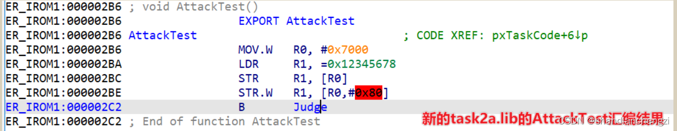
F5 The result of disassembly is shown in the figure below :

Next , First, ensure that the output can be correctly entered flag In the conditional branch of .
《ARM Cortex-M3 And Cortex Authoritative guide 》( Hereinafter referred to as the authoritative guide ), The first 11 The chapter is written with MPU Register related to locale , among 0xE000ED94 It's a register CTRL. According to the correspondence between static address and register , Predefined as follows :
#define MACRO_CTRL 0xE000ED94
#define MACRO_RNR 0xE000ED98
#define MACRO_RBAR 0xE000ED9C
#define MACRO_RASR 0xE000EDA0
then , stay vTaskStart Add the following lines of code to the , In order to access the register in the form of a pointer , And print all the original areas :
volatile unsigned int * pCTRL=(volatile unsigned int *)MACRO_CTRL;
volatile unsigned int * pRNR=(volatile unsigned int *)MACRO_RNR;
volatile unsigned int * pRBAR=(volatile unsigned int *)MACRO_RBAR;
volatile unsigned int * pRASR=(volatile unsigned int *)MACRO_RASR;
for(int i=0;i<8;i++){

	*pRNR=i;
	printf("%d,%d,%08x,%08x\n",*pRNR,*pCTRL,*pRBAR,*pRASR);
}
Registers have their own structure , Here we first define the structure 、 It would be more appropriate to define the structure pointer . however , Because the experimental task is simple , There is not much to change , So I just use unsigned integers to assign values .
To ensure that at least one MPU It's enabled , And then vTaskStart Add a line of code after the loop body in :
*pCTRL=5;
then Rebuild And run it directly , See where the exception is triggered , The results after running are shown in the figure below :

According to the teacher ,MemMange_Handler This exception will have a delay , So violation MPU The directive for zone protection is The above lines of code trigger the exception , Not the other code that follows . namely :
0x000002c2:  f44f 40e0  mov.w    r0, #0x7000
0x000002c6:  490c       ldr      r1, [pc, #0x30]
0x000002c8:  6001       str      r1, [r0]
0x000002ca:  f8c0 1080  str.w    r1, [r0, #0x80]
0x000002ce:  e7ec       b        #0x2aa
Corresponding AttackTest stay IDA Pro The assembly code in is as follows :
LDR Role of instructions : Store the memory address At the address indicated Successive 4 Bytes of data Transfer to destination register .
MOV.W	R0, #0x7000		;  take 0x7000 Assign a value to R0 register
LDR		  R1, =0x12345678    ;  take 0x12345678 Assign a value to R1 register
STR		  R1, [R0]		       ;  take R1 Continuity of 4 Bytes of data are transferred to R0 The address pointed to by the register
STR.W	  R1, [R0,#0x80]      ;  take R1 Continuity of 4 Bytes of data are transferred to (R0 The address that the register points to +0x80) in
B		  Judge			   ;  Jump to perform Judge
obviously , Visited #0x7000 and #0x7080 These two addresses , And both require write permission .
Analyze all the... Set by the teacher MPU Of RASR Of AP attribute , It can be seen that , Area 0、1、3 All read-only , Other areas are readable and writable to the privilege level , Area 6 and 7 There is no setting at present .AP The access permissions corresponding to the domain code are shown in the following figure ( From authoritative Guides ):

Combined base address RBAR and RASR Area size attribute in , It can be seen that ,#0x7000 and #0x7080 Both addresses are in the region 0 and 1 Inside , And they are not writable .
however , Except for these lines of instructions , There are other things you can't visit later ? Keep looking back .
Print flag The conditional branch of the function is as follows :

Which print flag The code corresponding to the conditional branch of is explained as follows :
1	ldr R0, #0x20000038	;  take 0x20000038 Assign a value to R0 register
2	ldr R1, [R0]		 ;  take R0 The value on the address pointed to by the register is read out and assigned to R1
3	adds R1, R1, #2		 ; R1 = R1 + 2, Affect carry flag bit C The addition operation of
4	str R1, [R0]		 ;  take R1 Continuity of 4 Bytes of data are transferred to R0 The address pointed to by the register
5	adr R0, aFlagU		;  Assign the address of the format string to R0
6	b.w __2printf	       ;  call __2printf
All in all ,Judge Memory addresses are also covered in 0xE000ED94 Read permissions and 0x20000038 Read and write permission of . Fortunately , adopt MPU We can see that ,0x20000038 Although in the area 2 Inside , But the area 2 read-write .0xE000ED94 Is not bound .
So these two addresses do not violate MPU Protected address .
In violation of the MPU Zone protection directive
Combine all the above analysis , You know , In violation of the MPU The directive for zone protection is AttackTest Function :
STR		  R1, [R0]		      ;  take R1 Continuity of 4 Bytes of data are transferred to R0 The address pointed to by the register
STR.W	  R1, [R0,#0x80]      ;  take R1 Continuity of 4 Bytes of data are transferred to (R0 The address that the register points to +0x80) in
Permissions violated
Yes 0x7000 and 0x7080 Write permissions for these two addresses .
relieve AttackTest Function violates new rules MPU Area reconfiguration code
in general , I added the release AttackTest Function violates new rules MPU Area reconfiguration codes are as follows :
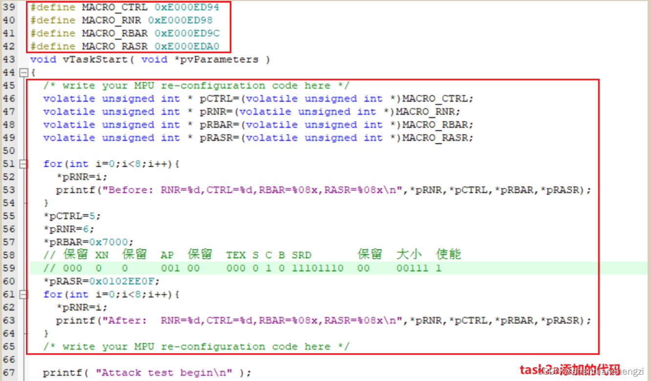
Run and get flag The results are as follows :

Description of the set area
CTRL
CTRL=5. To enable .
RNR
RNR=6, It means area 6.
In order not to overwrite the teacher's settings , I select the area 6 To configure new MPU Area .
RBSR
RBSR Set to 0x7000.
RBSR The structure of is as follows ( From authoritative Guides ):

The above table is very misleading , At first I thought ADDR It's independent , For example, when the address is 0x7000、 The area is 1 when , Corresponding ADDR Part of it is 0x7000, Corresponding RBAR yes 0x70001. Fortunately, a classmate woke me up in time , Look back at the authoritative guide , You will find that the address part is directly assigned , The last four digits were not considered at all .
After practice , The following conclusions can be drawn :
One side , When the penultimate digit VALID yes 0 When ,REGION Bit setting does not affect the modified MPU Area number register , The program will use MPU The area selected by the area number register , therefore The last four digits can be any value ;
On the other hand , The address must be REGION An integer multiple of the field size . First , We need to know Every bit of address can be indexed 8 Bits of data . For size 32B namely (32×8)bits The data of , In theory, you need to use l o g 2 ( 32 ) log_2(32) log2(32) position 、 That is to say 5 Bit address to represent , And every 4 Bit binary numbers correspond to one 16 Hexadecimal number . therefore , Use (00~1f) Can be said 32B The data of , And every 32B The interval between data , Should be 0x20.
REGION The minimum domain size is 32B, The address is N×0x20,N Integers . therefore , The minimum nonzero address is 0x20. Even if you directly order RBAR=0x20, Will not affect the countdown 5 Bit binary number setting .( amount to , Reciprocal 5 Bits are reserved bits , Just for convenience , So more definitions VALID Domain and REGION Domain )
Refer to the blog for the capacity corresponding to the address :【 Embedded foundation 】 Why? 0x100 yes 256 Bytes 、0x400 yes 1KB、0x800 yes 2KB、0x1000 yes 4KB?.
All in all ,RBSR=0x7000, It means MPU My base address is 0x7000.
RASR
RASR=0x0102EE0F, The corresponding attributes are as follows :
- AP = 001, Only privilege level reads are supported / Write ;
- TEX S C B = 000 0 1 0, Corresponding ROM, Flash( Programmable memory );
- SRD = 11101110, Corresponding sub areas 0 and 4 Enable , Other disabled ;
- Area size = 00111, Corresponding area size 256B;
- Can make = 1, Make this MPU It works .
Next, let's explain what I set up AP、SRD、 Area size 、 Why is the type the smallest :
AP
AP The corresponding relationship between code and access permission is shown in the following figure ( From authoritative Guides ):

As can be seen from the above table , Meet our privileged tasks 、 The minimum access required for read and write permissions is
001.Area size
The code of area size is shown in the figure below ( From authoritative Guides ):

Want to take the smallest , Then take it 32B, That is to say b00100. Unfortunately, I need to visit
0x7000and0x7080These two addresses , Take only 128B Neither. , Because take 128B、 The base address is 0x7000 When ,MPU The corresponding area is only0x7000~0x707F. So take 256B, Correspondingb00111.SRD
When the area size reaches 256B When , This MPU Large enough , Be able to set 8 Sub areas .
therefore , I also have to consider the sub region forbidden attribute SRD Set up .( I asked people , Others' lib Only one address was visited , Or the access address span is not so large . therefore , This is a special case )
My sub area 0 And subareas 4 Must be enabled , Everything else can be disabled .
So set to
11101110.type
Just a brief introduction to the major categories , incorrect TEX、S、C、B Give a detailed introduction .
This experiment involves TEX、S、C、B The settings of are shown in the figure below ( From authoritative Guides ):

obviously , Set to ROM,Flash Is the least privileged .
The subtasks 2 Unprotect a specific peripheral area and change the specified peripheral area to read / write
In subtask 1 Based on the analysis of , Don't need much explanation .
Plus the preset MPU It hasn't changed , So basically, just change the address range .
The experimental results are as follows .
Reverse analysis AttackTest function

In violation of the MPU Zone protection directive
AttackTest Medium STR R0, [R1].
Permissions violated
0x40010000 Write permission of .
relieve attackTest Function violates new rules MPU Area reconfiguration code
Code , And compare subtasks 1 Key changes to :

Running results :
Description of the set area
RNR=6.
CTRL=5.
RBSR Set to 0x40010000.
RASR=0x01020009, The corresponding attributes are as follows :
- AP = 001, Only privilege level reads are supported / Write ;
- TEX S C B = 000 0 1 0, Corresponding ROM, Flash( Programmable memory );
- SRD = 00000000, Area size does not reach 256B, Therefore, this attribute does not need to be configured ;
- Area size = 00100, Corresponding area size 32B;
- Can make = 1, Make this MPU It works .
边栏推荐
- 机器学习LDA——实验报告
- 10 years' experience in programmer career - for you who are confused
- Machine learning linear regression - Experimental Report
- Basic use of express in nodejs
- 请指教同花顺开户选选择哪家券商比较好?手机开户安全么?
- Is it safe to open an account in the top ten securities app rankings in China
- ACK攻击是什么意思?ACK攻击怎么防御?
- Easyx----- C language implementation 2048
- 量化初级 -- akshare获得股票代码,最简策略
- 【Redis 系列】redis 学习十六,redis 字典(map) 及其核心编码结构
猜你喜欢

代码规范 & 详细解释 husky、prettier、eslint、lint-staged 的作用和使用
02-Redis数据结构之链表

3、 Linked list exercise

【深度学习理论】(7) 长短时记忆网络 LSTM

FastRCNN

Solidworks渲染技巧如何不显示边线--显示样式设定
【深度学习理论】(6) 循环神经网络 RNN

19:第三章:开发通行证服务:2:在程序中,打通阿里云短信服务;(仅仅是打通阿里云短信服务器,不涉及具体的业务开发)

PC QQ hall upload update modify VersionInfo

深度理解STM32的串口实验(寄存器)【保姆级教程】
随机推荐
19:第三章:开发通行证服务:2:在程序中,打通阿里云短信服务;(仅仅是打通阿里云短信服务器,不涉及具体的业务开发)
Laravel-admin 登录添加图形验证码
Origin of b+ tree index
FastRCNN
express在nodejs中的基本使用
Laravel admin uses native JS to realize sound prompt and automatic playback
Grain Mall - distributed Foundation
动态规划解决股票问题(下)
Easyx-----c语言实现2048
机器学习线性回归——实验报告
代码规范 & 详细解释 husky、prettier、eslint、lint-staged 的作用和使用
Compréhension approfondie de l'expérience de port série stm32 (registre) [Tutoriel de niveau nounou]
Matlab programming example: how to count the number of elements in a cell array
有手就行的移动平均法、指数平滑法的Excel操作,用来时间序列预测
基于slate构建文档编辑器
ACK攻击是什么意思?ACK攻击怎么防御?
10 years' experience in programmer career - for you who are confused
在Oracle中update大量数据会不会导致undo空间爆掉
Is it safe to open an account in the top ten securities app rankings in China
PC QQ大厅 上传更新 修改versionInfo