当前位置:网站首页>Interpretation of key parameters in MOSFET device manual
Interpretation of key parameters in MOSFET device manual
2022-07-02 17:00:00 【Iron2222】
Write it at the front
I always thought , For electronic engineers , The best learning material is the data book of chips or electronic devices , It may be hard to read at first , But as long as you can hold on , And ask in a way that you don't understand , Will not check the attitude , believe me , It won't take long for you to see your progress .
So today I will take you to interpret a very common , But devices that seem to understand but not understand ——MOSFET, That's what we often say MOS Device manual of tube .
Interpretation object
Infineon NMOS:lRLML6346TRPbF.
The data manual can be downloaded at the following link :https://www.semiee.com/file/Infineon/Infineon-IRLML6346.pdf

But one thing needs to be explained in advance , Different manufacturers , Manuals for the same device are different , Especially some unimportant parameters , Some will not even provide , Everyone must pay attention to observation .
Key parameters and shape
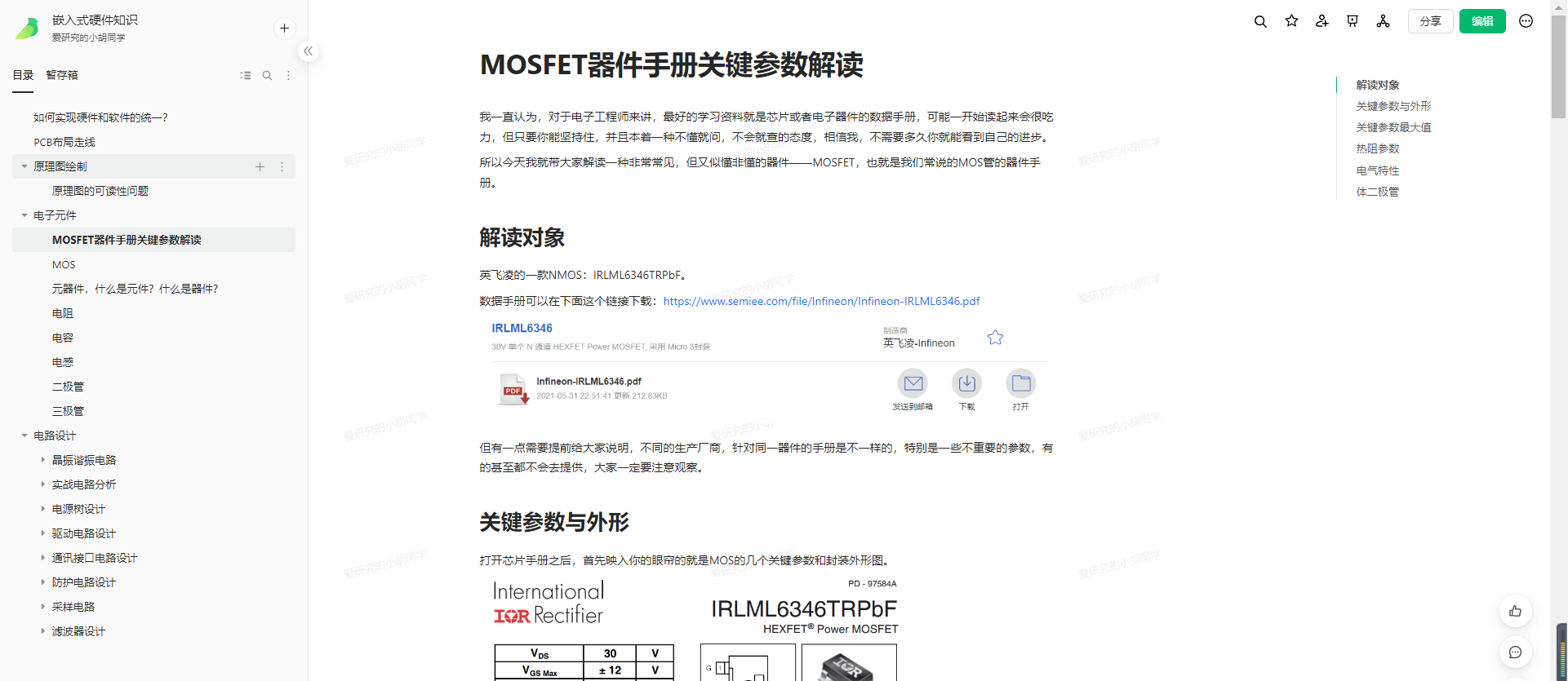
After opening the chip manual , The first thing that catches your eye is MOS Several key parameters and outline drawings of .

Here are several parameters that need your attention :VDS Leakage source voltage 、VGS Maximum value of grid source voltage 、RDS The maximum value of the conduction internal resistance ( Under different voltage conditions ). These parameters will be mentioned later , Later on .
On the right is the Internal schematic diagram and package model SOT-23.
Maximum value of key parameters
Further down you will see The maximum value of the six main parameters , This means that the device can operate at this value , But never exceed this value , Otherwise, the device will be damaged .

VDS Leakage source voltage 30V, This means that the maximum voltage you apply between the drain and the grid cannot exceed 30V;
ID Drain current value , The drain current values at the two backplane temperatures are given respectively , That is, the flow capacity of the drain , The maximum current that can flow , And the maximum flow capacity of the drain , It decreases with the increase of temperature ;
IDM Pulse peak , For power MOS Generally speaking, it has a strong peak flow capacity , The wiring between the connecting pin and the internal chip determines the size of this value ;
PD Maximum dissipation power , The dissipated power at two temperatures is given , The higher the temperature of the substrate , The lower the dissipated power ;
The following Linear derating factor , It means every degree of increase , Dissipated power decreases 0.01W;
VGS Voltage value between grid and source , No more than 12V;
TJ And TSTG The shell temperature and storage temperature that the device can withstand , Exceeding this temperature will make MOS The reliability of the tube decreases .
The extreme value of these key parameters is the limit that the device can withstand , Never exceed these values , At ordinary times, relevant allowance shall be reserved during type selection and design .
Thermal resistance parameters
Next you will see such a table , There are only two rows. , But it's very important .

This is the thermal resistance parameter from the device shell to the environment .
Of course, the premise is not to install radiators , When the device operates in the circulating air , How the shell temperature rises .
100 I mean , In the circulating air , The dissipation of power is 1W, There will be an ambient temperature that will make the shell temperature higher than the outside air 100 Centigrade .
Of course, the heat parameter should match the picture ~

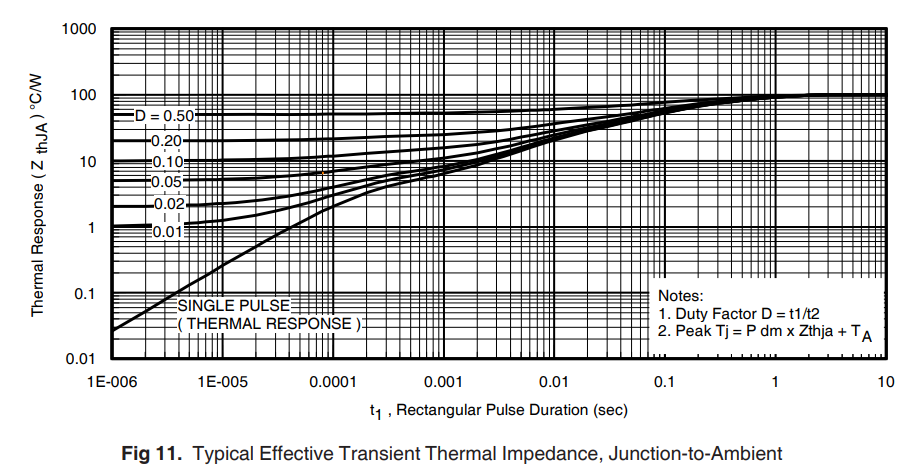
chart 9 Is the relationship between shell temperature and drain current , With the increase of shell temperature , The flow capacity of the drain decreases .
Electrical characteristics
following , Electrical characteristics .

There are many parameters in this table , Let's choose some important parameters to understand .
VDSS Withstand voltage between drain and source ;
RDS(ON) The conduction internal resistance of the device ;


These three figures , They are the changes of internal resistance of conduction under different conditions :
- The left one shows that the internal resistance of conduction is of positive temperature coefficient , As the temperature goes up , The greater the internal resistance of conduction ;
- In the middle is 2.5V And 4.5V Under driving voltage , The change of conduction internal resistance with drain current , Obviously, the driving voltage is high , The internal resistance of conduction is relatively small ;
- The right one indicates that under different shell temperatures , Increase the driving voltage , Change of conduction internal resistance , The lower the shell temperature is, the smaller the conduction internal resistance is .
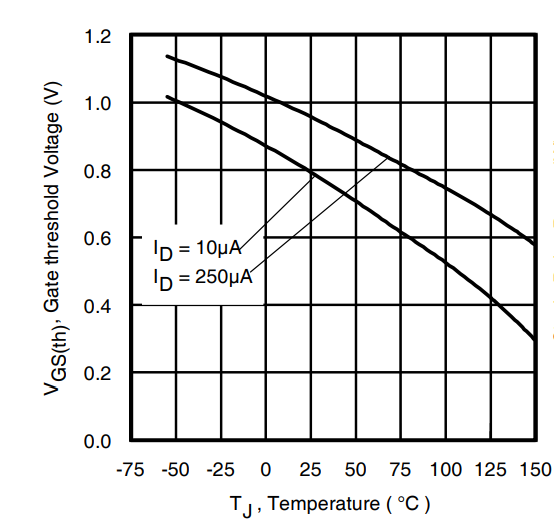
VGS(th) Gate threshold voltage ,0.8V That is to say, the grid can only reach 0.8V, The leakage source will start to have current flow ;
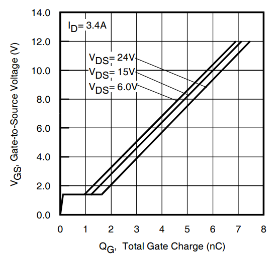
These two pictures are MOSFET The variation curve of the grid characteristics under different conditions , The left one is different VDS Under the condition of ,Vgs and Qg Corresponding relationship .

Qg,Qgs,Qgd, What we are most concerned about is Qg This parameter , It is the total charge of the grid , It has a large relationship with drive loss ;

t Those parameters are the rising and falling time of the switch , But this value is measured under specific conditions , When the external environment changes , These parameters will also change ;

C These parameters are parasitic capacitance , Our longest concern is Coss Output capacitance , Especially in LLC In resonant power supply , This parameter is very important .
Body diode

Is Current is the current that the body diode can conduct continuously , Maximum 1.3A;
Ism Is the pulse current flowing through the lifting diode , The biggest is 17A;
Vsd Forward voltage drop of bulk diode , Maximum 1.2V;
trr And Qrr They are reverse recovery time and reverse recovery charge ;
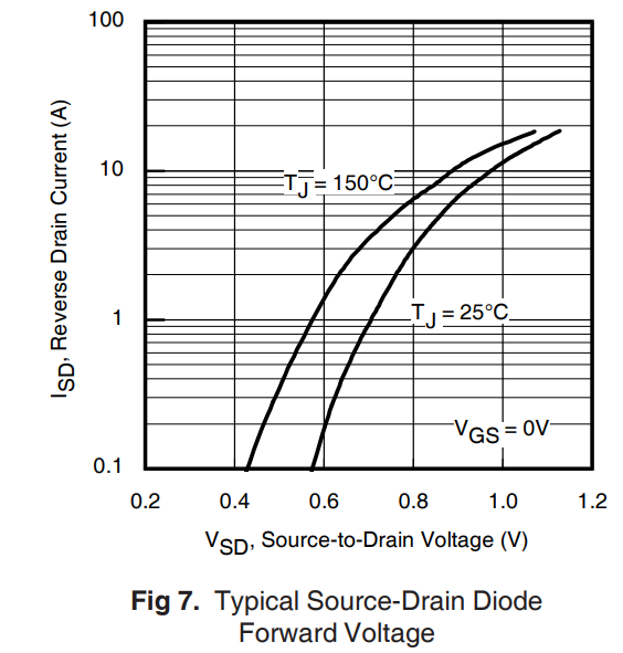

The first on the left is flowing Isd The greater the current ,Vsd And the bigger .
The first on the right is the schematic diagram of reverse recovery of body diode .
At the end :
Here, some common performance parameters are interpreted , This article is simply for everyone to know MOSFET What are the characteristic parameters , And have a simple understanding of these parameters , The specific and deeper ones are not stated .
The device manual is a little different from the chip data manual , There is no part involving circuit design , Next time I'll give you a manual to analyze a step-down chip , Focus on the construction of peripheral circuits .
by the way , I built a warehouse on YuQue , There are some hardware knowledge that I have recently sorted out and carried my personal notes , Students in need can have a look at . Embedded hardware knowledge · Language sparrow
边栏推荐
- ⌈ 2022 ⌋ how to use webp gracefully in projects
- LeetCode 2. Add two numbers
- Masa framework - DDD design (1)
- Machine learning perceptron model
- 移动应用性能工具探索之路
- 数字IC手撕代码--投票表决器
- R and rstudio download and installation tutorial (super detailed)
- unity Hub 登錄框變得很窄 無法登錄
- 电脑自带软件使图片底色变为透明(抠图白底)
- ROW_ NUMBER()、RANK()、DENSE_ Rank difference
猜你喜欢
PWM控制舵机

基于Impala的高性能数仓实践之执行引擎模块

七张图,学会做有价值的经营分析
Where can I open computer administrator permissions

Machine learning perceptron model
![[error record] the connection of the flutter device shows loading (disconnect | delete the shuttle/bin/cache/lockfile file)](/img/3f/79dcfcd88d779a5d493b4b539bd448.jpg)
[error record] the connection of the flutter device shows loading (disconnect | delete the shuttle/bin/cache/lockfile file)

只是巧合?苹果iOS16的神秘技术竟然与中国企业5年前产品一致!
linux下配置Mysql授权某个用户远程访问,不受ip限制
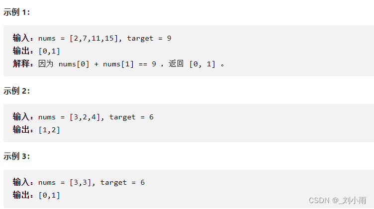
LeetCode 1. Sum of two numbers

LeetCode 2. Add two numbers
随机推荐
Atcoder beginer contest 169 (B, C, D unique decomposition, e mathematical analysis f (DP))
PCL least median square method fitting plane
Global and Chinese markets for slotting milling machines 2022-2028: Research Report on technology, participants, trends, market size and share
上传代码到远程仓库报错error: remote origin already exists.
LeetCode 5. Longest Palindromic Substring
LeetCode 6. Zigzag transformation (n-shaped transformation)
Configure ARP table entry restrictions and port security based on the interface (restrict users' private access to fool switches or illegal host access)
L'explosion de John utilise l'encodage d'entrée par défaut: UTF - 8 Loaded 1 password Hash (bcrypt [blowfish 32 / 64 X3])
Hard core! One configuration center for 8 classes!
SQL solves the problem of continuous login deformation holiday filtering
Ranger (I) preliminary perception
Cloud native cicd framework: Tekton
Classic quotations
LeetCode 1. Sum of two numbers
LeetCode 4. 寻找两个正序数组的中位数(hard)
P6774 [noi2020] tears in the era (block)
Kubernetes three open interfaces first sight
Leetcode1380: lucky numbers in matrix
Go zero micro service practical series (VIII. How to handle tens of thousands of order requests per second)
PWM breathing lamp