当前位置:网站首页>Use notes of Lichuang EDA
Use notes of Lichuang EDA
2022-07-26 18:54:00 【IOsetting】
Lichuang EDA
In Lichuang EDA Made on PCB You can import directly to jialichuang to place an order , Each registered user can place two free orders every month , Limit PCB Size 10CMx10CM, Five pieces per order , Even production to express all free , It is very suitable for making samples .
Lichuang website https://lceda.cn/,
SCH line
There is nothing to say about the circuit diagram , Make PCB The first important but easy step . Several points needing attention in the process
- Select the components of the appropriate pad
- General components are relatively simple , It depends on the pad size , 0805, 0603 perhaps 0402, Hand welded board to 0603 Just fine , 0402 Welding is more difficult , Because the components are too small , It is easy to be blown away or statically adsorbed by other objects .
- Power devices , LDO these , SOT89, SOT223, SOT23, Pay attention to the distinction , The size varies greatly , Avoid putting PCB It's inappropriate to come back and rework
- The layout of connecting devices is more diverse , One USB Type-B There are more than a dozen layouts , Remember the most commonly used , Otherwise PCB When I came back and found that the spare parts were inappropriate, I had to buy another one .
- stay PCB Under the area limitation , Try to choose the most versatile and easy to weld devices , For example, it is designed to 0805 The pad of the , Convenient welding , No, 0805 In the case of 0603 Can also paste .
- The order of needle arrangement function should refer to the design of similar common products , If there is a general order, use the general order , The daily habit of wiring is not easy to change , Unification can reduce the risk of errors .
- In order to make the circuit diagram more concise ( Avoid winding ), Most circuits will use Net Label Formal annotation , At this time, pay attention to distinguish
- Just connect , If the intersection is connected, there will be a dot
Shortcut key
- Move the canvas : Right click and drag
- Zoom in and out : Mouse wheel
- Rotating element : Click and then click the blank , or
R - attachment :
W, PressEscsign out
PCB
Edit according to the layer
- Similar to other drawing software . When switching to pads or components existing in the current layer , Will highlight , Others darken .
- The more important thing is the front , Back ( double PCB), Outer frame These three floors
- After selecting a layer , Press
Shift+SYou can hide other layers , It is convenient to modify on the current layer - Press
KYou can immediately adjust the size to adaptive
Company
Click... In the blank space without components , Units can be selected in the right attribute bar , mm, mil, 100mil=2.54mm
PCB Board size
Switch to the outer frame layer
- In this layer , Just draw lines in the normal way , PCB During production, it will make plates according to this size
- Click twice on the side , You can select this edge individually , Modify the position through attributes
put
Press space or R, Can rotate components
wiring
After the components are placed and fixed , Click the wiring icon , Or press the shortcut key W Wiring
Basic operation
- Wiring angle : Oblique line 45°, Go at an obtuse angle , Do not have right angles or acute angles
- Wiring width : Before the connection ends , Press
TabKey can modify the width . The minimum use of signal line 6mil, It's usually 10mil, Power cord recommendations 15mil above - Error message : If wiring violates the default rules , There will be X Tips , Need modification
- modify :
- Click to select the line , Point in the center line of the point , Will only move this point ( The points on both sides don't move , Adjust the angle and length )
- Click to select the line , Press and hold the line , Will move the middle edge with two points ( Keep the angle , Adjusting position )
- Click to select the line , Three strikes hit the middle of the line , You can add a little
- Point in the line , Three clicks can delete
- GND: No wiring , Leave the last copper
- Cloth thread , Will take it net identification , Zoom in to a certain multiple to see , At this time, the benefits of high-resolution display are shown
- from SCH to update PCB when , Wired net Not necessarily updated , If you still keep the original net identification , There will be ratline
Through hole
- When the connection is blocked , It can be connected through a through hole .
- First draw a line through the hole , Then point a via on the line , Then cloth the other side
- After wiring , You can add a through hole in the copper area , Strengthen ground wire connectivity ( Avoid capacitive effects )
Fly line ratline
- Flywires are used to indicate the connectivity between pads
- After wiring connection , The flying line between the two pads will disappear
- After all connections are completed ( Including copper coating ), The straight lines between the pads should all disappear , If there is still , It means that this part has not been wired
- You can select from the object type in the tool box , Display only ratline Check all flying lines , Convenient for inspection
moisturize Teardrop
- After all connections are completed , It can be used TearDrop Moisten the wiring between the wiring and the pad to avoid right angles
- If copper has been applied , Copper coating will be automatically adjusted after wetting
- Teardrop Also bring net identification , But it is often covered by components and cannot be found intuitively , If you want to modify the wiring , It is recommended to hide components first , Then put the... On the pad to be changed Teardrop First delete
Copper coating
- Select the layer , Click the dotted copper coating button in the tool set , Then select the box PCB peripheral , After the box ( You can see the dotted line changes ), Then press Esc, Copper will be applied to the selected area in this layer .
- The double-layer board needs to be coated with copper on both sides
- In global settings , Set the copper coating invisible ( Show only borders ), It is recommended to hide the copper coating when modifying the wiring
- Click the dotted box with copper , You can adjust the connection mode of copper coating on this side and bonding pad , Divergent or direct connection , Direct connection will not leave a gap
- After circuit modification , Re moisten (Teardrop), It will automatically reapply copper , You can also click the button to reapply copper
Silk screen
Click on T Tools , You can add text
Delete component ID in batch
The identification of components has several parts : Component name , Component number , And the silk screen of the pad outline . The first two can be hidden in the settings , Will not appear in the final PCB Yes .
Right click on the component , Select a similar type , In the attribute box on the right , Set the identification and number to not display , It's all hidden ( There will be no silk screen printing when making )
3D preview
Generate 3D preview , intuitive , You can see the spacing between components , Whether the arrangement is too dense , Is there any overlap , Check whether the silk screen printing is correct, etc . Some low-level mistakes can be avoided .
modify
- When modifying , If the wiring diagram changes , First from SCHEMATICS Change , And then again Update To PCB
- Wiring and vias , Including the edges produced by wetting , All have Net Name , Modify the line , For example, after switching the order of needle arrangement , Of these components Net label Maybe it's wrong , Need modification , Otherwise, errors will be displayed or generated ratline
- moisturize (TearDrop) The resulting edge may not be easy to spot under the pad , You can hide components , Replace these small components Net Label. Or in TearDrop Set delete... In the dialog box , Do it uniformly after the modification TearDrop
- Last in ratlines( Fly line ) On the floor
Shift+SHide other layers , See if there are any untreated flying lines
Video learning : https://www.bilibili.com/video/BV1dU4y187fN
Work recommendation
STM32 Development board series
- https://oshwhub.com/spadger/bluepill
Spadger Of STM32F103C8T6 Core board , MicroUSB, LDO It uses a less common SE8533 - STM32F103C8T6 Core board https://oshwhub.com/baobaoa/bluepill
Baobaoa stay Spadger Based on the modified version of the project , USB Change it to Type-C, LDO Change it to SOT89 Of AMS1117
边栏推荐
- Brand new! Uncover the promotion route of Ali P5 Engineer ~p8 architect
- Redis core principles
- mpc5744p的pit报错, RTOS无法启动, 时钟源问题
- MySQL - 函数及约束命令
- 开发winform中遇到的一些问题汇总(持续跟新)
- 常用功能的测试用例
- 工赋开发者社区 | 定了!就在7月30日!
- File upload and download test point
- Vector CANape - How to Send Receive CAN Message in CANape
- "Wei Lai Cup" 2022 Niuke summer multi school training camp 3 record
猜你喜欢

一文详解MES系统给企业带来的5大好处,附应用场景

微软默默给 curl 捐赠一万美元,半年后才通知

NFT digital collection system development: sold out when online, and netizens "spike" Digital Collections

2022上海市安全员C证操作证考试题库模拟考试平台操作
![[soft exam] soft exam tutorial + real questions over the years](/img/91/72cdea3eb3f61315595330d2c9016d.png)
[soft exam] soft exam tutorial + real questions over the years

Sentinel 隔离与降级

【考研词汇训练营】Day 14 —— panini,predict,access,apologize,sense,transport,aggregation

Still using xshell? Recommend this more modern terminal connection tool
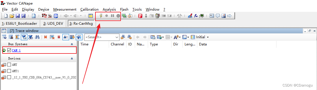
Vector CANape - How to Send Receive CAN Message in CANape
Operations research 69 | explanation of classic examples of dynamic planning
随机推荐
NFT数字藏品系统开发:上线即售罄,网民“秒杀”数字藏品
SSM整合-异常处理器和项目异常处理方案
2022年云商店联合营销市场发展基金(MDF)介绍
Seata 入门简介
详细介绍@GetMapping和@PostMapping的区别
Neural network learning (2) introduction 2
PyQt5快速开发与实战 3.5 菜单栏与工具栏
Vector canoe menu plugin getting started
凝心聚力,心心向印!印度中资手机企业协会(CMA)正式运营!
Linear regression -- Taking an arithmetic sequence as an example
rancher部署kubernetes集群
模块八作业 - 消息数据 MySQL 表设计
Exploratory software testing
455. 分发饼干【双指针 ++i、++j】
5款WPS Office最佳海外替代品
Operation: skillfully use MySQL master-slave replication delay to save erroneously deleted data
议程速递 | 7月27日分论坛议程一览
这场竞赛,能读懂题目的你大有可为
Download and configuration of irrklang audio library
Ministry of Finance: IC design enterprises and software enterprises will be exempted from corporate income tax this year and next!