当前位置:网站首页>FPGA interview notes (II) -- synchronous asynchronous D flip-flop, static and dynamic timing analysis, frequency division design, retiming
FPGA interview notes (II) -- synchronous asynchronous D flip-flop, static and dynamic timing analysis, frequency division design, retiming
2022-06-11 06:06:00 【Fighting_ XH】
List of articles
- 1、 Behavior level and RTL The difference between grades
- 2、 About LUT
- 3、`include And conditional compilation
- 4、 Write asynchrony D trigger ( Yangzhi electronic written test )
- 5、 static state 、 Advantages and disadvantages of dynamic timing analysis ( via VIA 2003.11.06 Shanghai written examination questions )
- 6、 Use one out of two multiplexers mux2 and inv Not gates implement XOR operations ( philips - Datang written examination )
- 7、 The difference between registers and latches , Why use more registers , How the latch is generated in the behavior level description
- 8、 D Trigger implementation 2 Frequency division Verilog describe ( Han Wang written examination )
- 9、D The flip-flop realizes the circuit of frequency division with synchronous high set and asynchronous high reset end
- 10、 Design a preset initial value 7 Binary cycle counter
- 11、 High resistance state
- 12、 Yes Retiming The understanding of Technology
FPGA A summary of the basics
1、 Behavior level and RTL The difference between grades
The process of digital system design :
Algorithm —— Behavior level description ——RTL Level description —— Gate level grid —— Physical layout
1.1 RTL level ( It can be integrated into gate level circuit )
- RTL Level is also called register level , It refers to the way to describe the circuit data flow with registers , Using hardware description language (verilog) describe , Statements must be comprehensive ( It can generate various gate circuits ).
- Register and combinational logic RTL level . stay RTL Lower level , Need to describe all levels of registers ( register ), It also describes the signal conversion relationship between registers at all levels ( Combinatorial logic )
- Need to know how to use RTL Stage describes the schematic diagram of the pipeline , Also know where to use combinatorial logic , Where registers are needed , And how to achieve .
1.2 Behavior level
- The behavior level is generally based on algorithms , It is only used to describe the function of the circuit , The ultimate goal is to get the relationship between input and output , Adopt any verilog Grammar description is OK , Because there is no need to consider the comprehensive problems .
- Behavior level description , Generally, direct assignment is adopted , A great deal of arithmetic is required 、 Delay 、initial Block, etc , Therefore, it is often used in verification simulation .
subject :Verilog The level of language corresponds to (D)
A. The system level , Behavior level , Functional level , Register transfer level , Gate level
B. The system level , Behavior level , Register transfer level , Functional level , Gate level
C. The system level , Functional level , Register transfer level , Behavior level , Gate level
D. The system level , Functional level , Behavior level , Register transfer level , Gate level
A detailed explanation of the difference between the two
2、 About LUT
2.1 LUT What is it?
LUT For lookup table , seeing the name of a thing one thinks of its function , Its fundamental function is to find ( For example, we look up the word we want in the dictionary ). The essence : Given an input value , Return to a corresponding output value .
2.2 N Dimension lookup table
The lookup table includes one dimension (1D LUT)、 Two dimensional lookup table, etc .
- (1D LUT) One dimensional lookup table Is in one-dimensional space , Given an input variable , Get a corresponding output variable . As shown below , Give input 0, Get the output 0, Give input 1, Get the output 0.5……

- (2D LUT) Two dimensional lookup table In two-dimensional space , Input input two unrelated variables , Will get the corresponding output . For example , Our input is a set of coordinates (x, y), The corresponding value of this coordinate can be obtained .
- Empathy ,3D LUT Namely 3D lookup table , Enter three unrelated variables , Get an output value . Can be found in Application in color space , For example, give a group RGB The numerical , After searching through the lookup table , Get a new set of RGB The number , Thus, the color change is realized .
2.3 FPGA Medium LUT
FPGA The essence of a lookup table is RAM, every last LUT It can be regarded as a 4 Bit address line 16*1RAM. In general, we use LUT4 perhaps LUT6, Because if the input digits of the lookup table are too large , Cascade operation is required , It will cause greater data transmission delay ;
stay FPGA in , Can make use LUT To realize the function of combinational logic circuit , Form a gate circuit .LUT The data stored in is a truth table , According to the result of logical calculation , Can be in LUT Find the corresponding content in .
- As follows, we implement a two input lookup table , Through two unrelated inputs , Get the corresponding output according to the logic function , The logical function here is to look up the table , Therefore, the lookup table is also equivalent to the truth table of logic gates .
module test(
    input  a,
	 input  b,
	 output out1,
	 output out2
	 );
	 assign out1 = a & b;
	 assign out2 = a | b;
endmodule
It can be seen that we adopt LUT The gate circuit is realized ,LUT Inside is the truth table of logic gate circuit .
according to LUT yes ROM And the internal storage data is the essence of truth table , about LUT1, We can enter variables 00, Output LUT1 Address in 00 The value in the storage unit 0……
- How to see how many lookup tables are included in a design ?
3.2.2 Detailed explanation
LUT The past and the present
FPGA in LUT Detailed explanation
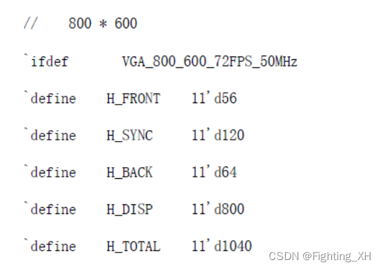
3、`include And conditional compilation
We use it `include To include the file , and C Language is similar to , This file defines some common macro parameters . One include Only one header file can be included .
- Conditional compilation : Compile a set of statements when conditions are met , When the conditions are not met, another group of statements will be compiled .
- `define As a sign of conditional compilation , Define which section and which section can be compiled , Otherwise, do not compile .
- `ifdef Can appear anywhere in the design ;
 `ifdef  Macro name ( identifier )  Procedures section 1 `else
         Procedures section 2
`endif
stay FPGA Image processing ,VGA The driver design office will use this method of conditional compilation , Used to select different VGA The corresponding display leading edge in the resolution 、 Line valid macro parameters , The following is the definition 800*600 Resolution VGA Timing parameters . We do this by including header files ( It is recommended that the header file and this file be in the same folder ) And with `define To select the corresponding resolution .
`define VGA_800_600…… It means 800*600 Part of the resolution code is compiled .
4、 Write asynchrony D trigger ( Yangzhi electronic written test )
About D trigger :
D The trigger is usually on the rising edge of the clock , This captures D The value entered at the end , Then leave the value unchanged , Until the next rising edge comes , Recapture D Input value of the end . So it has the function of storing and memorizing .
Be careful :D The normal operation of the trigger must meet the requirements of its holding and establishment time . If the data does not meet the requirements when it is stable , It cannot be stored normally .
// a   asynchronous D trigger
 module test(clk,rst,d,q);

	 input clk;
	 input rst;
	 input d;
	 output reg q;

[email protected](posedge clk or negedge rst)
	 if(!rst)
	     q <= 0;
	 else
	     q <= d;

endmodule
Generated RTL as follows :
4.1 Octet synchronization D trigger
 module test(clk,rst,d,q);

	 input clk;
	 input rst;
	 input [7:0]d;
	 output reg [7:0]q;

[email protected](posedge clk )
	 if(!rst)
	     q <= 0;
	 else
	     q <= d;

endmodule
RTL chart :

4.2 With asynchronous reset , Synchronous reset signal function D trigger
module test(clk,rst,clr,q,d);


	 input           clk    ;
	 input           rst    ;
	 input clr;
	 input           d      ;
	 output  reg     q      ;


always @ (posedge clk or posedge clr )
    if(clr)
        q <= 0;
    else if(rst)
	     q <= 1;

    else
	     q <= d;

endmodule

This is equivalent to having priority , Clear signal clr Priority over reset rst The signal .
Priority understanding : When clr When clearing , No matter rst Whether the signal is high level or low level will not affect q by 0 Result .
5、 static state 、 Advantages and disadvantages of dynamic timing analysis ( via VIA 2003.11.06 Shanghai written examination questions )
1、 Dynamic timing analysis : It is what we usually call simulation , The simulation can verify the function and timing . Method : First determine the test vector , Enter the hardware model , Conduct simulation .
advantage : More accurate , Compared with static timing , It applies to more design types .
shortcoming : In case of door level, etc , Slow analysis ; Second, it requires the use of input vectors , This makes it possible to omit some critical paths in the analysis process , It is difficult to ensure adequate coverage ; As the scale grows , The number of vectors required grows exponentially .
2、 Static time series analysis : Only time series can be analyzed , No functional verification .
advantage : There is no need to enter a test vector , Much faster than dynamic timing analysis , Improve simulation time . Use the method of exhaustive analysis , Each path can be verified (100% Cover ), Analyze the propagation delay on the path , For example, combinational logic delay 、 Wiring delay, etc , Check whether the signal establishment time and holding time meet the timing requirements . Through the analysis of maximum path delay and minimum path delay , Identify errors that violate timing constraints . Very fast 、 Less memory . Time sequence analysis results can be used for time sequence optimization .
shortcoming : Static timing analysis can only analyze synchronous circuits , It is impossible to analyze the timing of asynchronous circuits . Under deep submicron process conditions , Static timing analysis cannot completely include all the factors that affect the delay .
6、 Use one out of two multiplexers mux2 and inv Not gates implement XOR operations ( philips - Datang written examination )
module test(sel,b,c);
	 input   sel ;
	 input   b   ;
	 output  c   ;

   assign  c= sel ?(~b):(b);
endmodule
Generated RTL chart :
Use only mux Implement XOR :
7、 The difference between registers and latches , Why use more registers , How the latch is generated in the behavior level description
1、 Latch Latch : Latches are level triggered , It belongs to asynchronous circuit design .———— For combinational logic
shortcoming : It's not good for timing analysis ; Sensitive to burrs ;FPGA There is no latch unit , It consists of lookup tables and triggers , Therefore, more resources will be wasted .
Several conditions that generate latches :
1,case—— The lack of default A latch is generated when
2,if-------else if —— The lack of else A latch is generated when
3,[email protected]( Sensitive signal table )—— If the signal participating in the assignment on the right side of the assignment expression does not appear in the sensitive list, a transparent latch will appear
2、 register Register: The register is the clock edge trigger mode , It belongs to synchronous circuit design .—— For sequential logic
Registers are better for timing analysis , It can also prevent metastable state and other phenomena ,FPGA There are register units in the , Therefore, chip resources can be saved by using .
8、 D Trigger implementation 2 Frequency division Verilog describe ( Han Wang written examination )
Reference for frequency division design and simulation
verilog Code :
module test(clk,rst_n,out);

	 input   clk ;
	 input   rst_n ;
	 output  reg out;


always @ (posedge clk or negedge rst_n)
    if(!rst_n)
	     out <= 0;
	 else
	     out <= ~out;
endmodule
RTL chart :
tb file :
`timescale 1ns/1ns `define clock_period  20
module test_tb;

	   reg clk;
		reg rst_n;

		wire out;


	  test  u1(

	   .clk(clk),
	   .rst_n(rst_n),
		.out(out)

	 );

// Generate clock reset excitation
	 initial  clk = 1;
	 always #(`clock_period/2) clk =~clk;

initial  begin
	 rst_n = 0;
	 #5;
	 rst_n = 1;
	 #100;
	 $stop;
	 end


endmodule
Waveform simulation :
9、D The flip-flop realizes the circuit of frequency division with synchronous high set and asynchronous high reset end
There are two points to focus on : Synchronous high set and asynchronous high reset .
So there are two signals, set and reset ——set and rst
verilog The code is as follows :
module test(clk,rst,set,q);


	 input           clk    ;
	 input           rst    ;
	 input           set   ;
	 output  reg     q ;


always @ (posedge clk or posedge rst )
    if(rst)
	     q <= 0;
	 else if(set)
	     q <= 1;
    else
	     q <= ~q;

endmodule
RTL chart :
10、 Design a preset initial value 7 Binary cycle counter
module test(clk,rst_n,load,data,cout);


	 input           clk    ;
	 input           rst_n  ;
	 input           load   ;
	 input       [2:0] data ;
	 output  reg [2:0] cout  ;


always @ (posedge clk )
    if(!rst_n)
	     cout <= 3'd0; else if(load) cout <= data; else if(cout == 3'd6)
	     cout <= 3'd0; else cout <= cout + 3'd1;

endmodule
If you want to design a preset initial value 15 Binary cycle counter , Modify the bit width and the maximum count .
11、 High resistance state
High resistance state refers to an output state of a circuit , Same as high and low level , But it is neither high nor low , If the high resistance state is input to the next circuit , It has no effect on the lower level circuit , It can be understood as an open circuit , Not driven by anything , It doesn't drive anything .
12、 Yes Retiming The understanding of Technology
Retime (Retiming) It is a timing optimization technology , Used without affecting the circuit input / Output behavior across combinational logic registers thus improves design performance .
for example : When combinatorial logic is too large , We can use assembly line to exchange area for speed —— Insert register 

边栏推荐
- 安装Oracle数据库
- Fix Yum dependency conflict
- Yoyov5's tricks | [trick8] image sampling strategy -- Sampling by the weight of each category of the dataset
- Login and registration based on servlet, JSP and MySQL
- Sword finger offer 32: print binary tree from top to bottom
- ThymeleafEngine模板引擎
- Altiumdesigner2020 import 3D body SolidWorks 3D model
- Clojure installation of metabase source code secondary development
- Use com youth. banner. Solution to the inflateexception reported by the banner plug-in
- FPGA面试题目笔记(三)——跨时钟域中握手信号同步的实现、任意分频、进制转换、RAM存储器等、原码反码和补码
猜你喜欢

Warmly celebrate that yeyanxiu, senior consultant of Longzhi, won the title of "atlassian Certified Expert"

Free get | full function version of version control software

NFC Development -- difference between ID card and IC card (M1 card and CPU card) (III)

Sqli-labs less-01

Matlab实现均值滤波与FPGA进行对比,并采用modelsim波形仿真

Write a list with kotlin

Altiumdesigner2020 import 3D body SolidWorks 3D model
Don't be afraid of xxE vulnerabilities: understand their ferocity and detection methods

View controller and navigation mode
![[IOS development interview] operating system learning notes](/img/1d/2ec6857c833de00923d791f3a34f53.jpg)
[IOS development interview] operating system learning notes
随机推荐
FPGA设计中提高工作频率及降低功耗题目合集
This is probably the most comprehensive project about Twitter information crawler search on the Chinese Internet
Which company is better in JIRA organizational structure management?
Analyze the capacity expansion mechanism of ArrayList
Fix [no Internet, security] problem
Gilde failed to go to the listener to call back the reason record when loading the Gaussian blur image
Sign for this "plug-in" before returning home for the new year
qmake 实现QT工程pro脚本转vs解决方案
Set the IP address using batch
All the benefits of ci/cd, but greener
How to use the markdown editor
NLP-D46-nlp比赛D15
Principle of copyonwritearraylist copy on write
ELK日志系统实战(六):技术选型之vector与filebeat对比
做亚马逊测评要了解的知识点有哪些?
Concepts and differences of parallel computing, distributed computing and cluster (to be updated for beginners)
Utiliser le fichier Batch Enum
Database basic instruction set
NFC Development -- difference between ID card and IC card (M1 card and CPU card) (III)
Distributed framework ray - detailed introduction to starting ray and connecting clusters