当前位置:网站首页>[little knowledge] PCB proofing process
[little knowledge] PCB proofing process
2022-06-25 07:48:00 【PCBA chengyaoer】
do pcb The purpose of proofing is to prepare the product before mass production , First make a small number of samples to test whether the product quality is qualified , To some extent, it can avoid risks for future mass production . that ,PCB What is the PCB proofing process ?

More content can be seen in official account. :PCBA Information sharing
First step : Check the data
Before production ,PCB The circuit board factory will check the board making data provided by the customer , Including the size of the board 、 Process requirements, product quantity and other relevant data , The next step of production can only be carried out after reaching an agreement with the customer .
The second step : Open the material
According to the information provided by the customer , On a plate that meets the requirements , Cut off small pieces to produce panels . Specific operation : Big board → Press MI Cutting plate is required → Curium board → Beer fillet / Edging → Out of the board .
The third step : drill hole
stay PCB Drill the required hole diameter at the corresponding position of the circuit board . Big board → Press MI Cutting plate is required → Curium board → Beer fillet / Edging → Out of the board .
Step four : Heavy copper
A thin layer of copper is chemically deposited on the insulating hole . Specific operation : Rough grind → Hanging board → Automatic copper wire → Lower board → Soak 1% rare H2SO4→ Thicken the copper .
Step five : Graphic transfer
Transfer the image on the production film to the board . Specific operation : Hemp board → Pressure film → Standing → Counterpoint → Exposure → Standing → Rush to the shadow → Check .
Step six : Pattern plating
Electroplate a copper layer with required thickness and a gold nickel or tin layer with required thickness on the exposed copper skin or hole wall of the circuit pattern . Specific operation : Board up → Degreasing → Wash twice with water → Micro erosion → Wash with water → pickling → Copper plating → Wash with water → Pickling → Tinning → Wash with water → Lower board .
Step seven : Retreat the membrane
Apply the anti electroplating coating with NaOH Solution removal , Expose the non circuit copper layer .
Step eight : etching
Remove the non circuit parts with chemical reagent copper .
Step nine : Green
Transfer the green film graphics to the board , It mainly protects the circuit and prevents tin on the circuit when welding parts .
Step 10 : character
stay PCB Legible characters are printed on the board . Specific operation : After the green oil finally curium → Cool and let stand → Adjust the net → Print characters → Rear curium .
Step 11 : Gilded fingers
Coat the plug finger with nickel of the required thickness / Gold layer , Make it more hardness and wear resistance .
The twelfth step : forming
The customer needs the shape with the die stamping or CNC gongs machine gongs .
Thirteenth Step : test
It is not easy to find by visual inspection because of an open circuit 、 Functional defects caused by short circuit, etc , It can be tested by flying needle tester .
The above is pcb The process of circuit board proofing , I hope it helped you !
More content can be seen in official account. :PCBA Information sharing
边栏推荐
- 【日常训练】207. 课程表
- VectorDraw Developer Framework 10.10
- Home environment monitoring system design (PC version) (mobile app version to be determined)
- OpenCV每日函数 结构分析和形状描述符(8) fitLine函数 拟合直线
- Chuantu microelectronics breaks through the high-end isolator analog chip market with ca-is3062w
- npm install 报错 : gyp ERR! configure error
- OpenMP入门
- 机器学习笔记 - 时间序列的线性回归
- CPDA | how to start the growth path of data analysts?
- 1742. 盒子中小球的最大数量
猜你喜欢
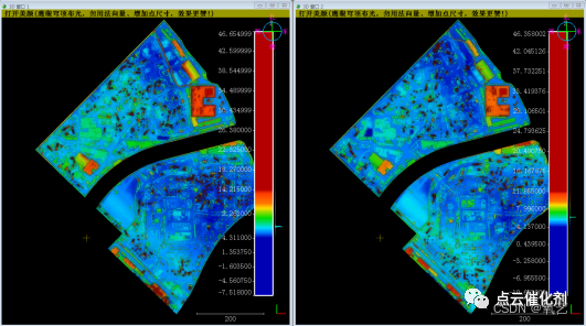
"Spatial transformation" significantly improves the quality of ground point extraction of cliff point cloud

Find out what informatization is, and let enterprises embark on the right path of transformation and upgrading
VectorDraw Web Library 10.10

Estimation of dense forest volume based on LIDAR point cloud with few ground points

Terms and concepts related to authority and authentication system

STL tutorial 4- input / output stream and object serialization
搞清信息化是什么,让企业转型升级走上正确的道路
点云智绘在智慧工地中的应用
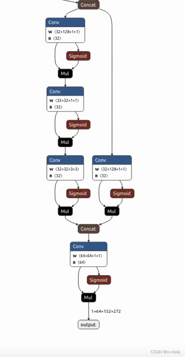
FairMOT yolov5s转onnx
Tupu software digital twin 3D wind farm, offshore wind power of smart wind power
随机推荐
smartBugs安装小问题总结
Introduction to Sichuan Tuwei ca-is3082w isolated rs-485/rs-422 transceiver
双三次差值bicubic
What if there is no point in data visualization?
Accès à la boîte aux lettres du nom de domaine Lead à l'étranger
Application scheme | application of Sichuan earth microelectronics ca-is398x in PLC field
Bicubic difference
Access to foreign lead domain name mailbox
基于激光雷达的林业调查常用术语及含义锦集
ts环境搭建
Different paths ii[dynamic planning improvement for DFS]
Tupu software digital twin 3D wind farm, offshore wind power of smart wind power
【视频】ffplay 使用mjpeg格式播放usb摄像头
Misunderstanding of switching triode
VOCALOID笔记
权限、认证系统相关名词概念
力扣76题,最小覆盖字串
57. 插入区间
el-input实现尾部加字
Sichuan earth microelectronics 8-channel isolated digital input receiver