当前位置:网站首页>Schematic drawing for pads
Schematic drawing for pads
2022-06-11 12:39:00 【Zhaokaixin xiansen】
First, create a directory of new projects on our computer , For example, the directory shown in the figure below .
among LIB It is used to save our encapsulation library ,PCB For preservation pcb file ,SCH Used to save schematic files . After creation , We began to work on the circuit board .
Start by opening PADS Logic Software .
Click New in the upper left corner to start creating a schematic file .

Click ok . You can save it , Save to the folder we created before .
As shown in the figure below . Even if the schematic file is created , Now start to draw the schematic diagram 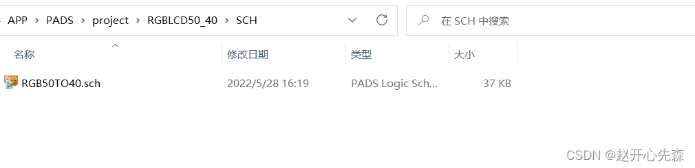
Click Library , Create a device library for our project .
After creation , Click manage library list to put our library file at the top .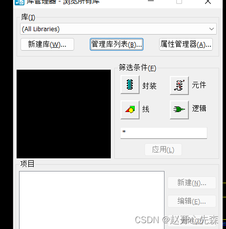
The following figure shows the library I use here .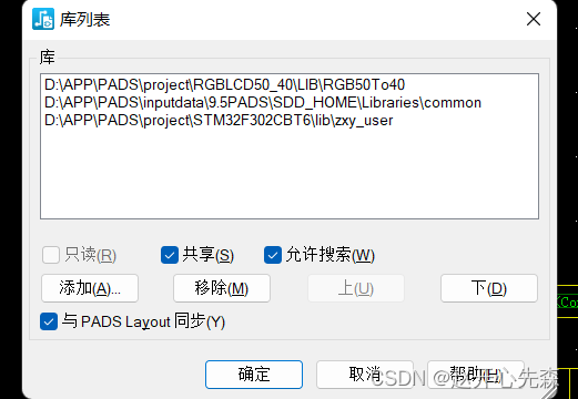
Click component editor under tools , Draw the originals we need 
Because I am here to do a RGB Screen line sequence adapter board , take 50pin Conversion of 40pin, So let's draw a 50pin My seat , See the following figure after entering . First use g 100 Set the grid to 100, Reuse gd 100 Set the display grid to 100
Use here to start adding pins 
Start editing electrical parameters after exiting 
The pins are renumbered here .
You can also click Edit graphic to return to the graphic editing interface .
Here we use create 2D Draw a box with a line .
After modification, we exit the component editor . Then add it first to see what the effect is .
Click Add component .
It can be seen that there is no pin description , I also feel that this box is a little big , So let's revise again .
Right click the pop-up option in the blank space and select select component , Then select our , Then click Edit component , Go to the next page and click Edit graphic . Then add a name to the pin .
Then the figure is drawn , We also need to add cpb encapsulation , open PADS Layout
Then click... In the tool PCB Package editor , Here's the picture 
Here we switch to millimeter units and use the modeless command umm You can add pads by doing the following 
Right click to select padset padstack 
We now combine the parameters of this device to complete this PCB encapsulation 
Modify padstack parameters as follows 
The width is the width of the device , The length is as follows, and then add 0.5mm The compensation value of 
Set the first padstack information as follows ,
The calculation is as follows ,x The coordinates are three pins in total , Two spaces ,2* 0.95( Pin spacing )/2=0.95,y coordinate :2.6 + 0.5( Compensation pin ) - 0.5( One pin length )/2=1.3, After setting the first one , Then step by step and repeat to get the other two , Then use the third pin , Use step-by-step and repeat to get the 4 individual , Up and then spaced 2.6.
Then use the 4 One is shown in the figure below , Get everything 6 A pin 
As shown in the figure below , This makes it easy to package .
We then added a frame to make him look better .
As shown in the figure below , Add another dot , Express 1 Position of pin No .
Then put our frames on the screen printing layer , Right click the blank space and select the shape , Then select the frame we draw , Then select the layer in the following figure .
You need to select the options shown in the following figure 
It's better to package and make in this way , Then the schematic diagram is made . After the schematic diagram is made , Let's check the schematic diagram with the following options 
Generally, it is OK to see if it is not used , Determine whether the lower pins are used correctly . After confirmation, you can send the net list to pcb 了 , First click the options shown in the following figure 
The following interface will appear .
Design options remove options 
Modify the preferences as follows , Others remain default 
So it's set up , Then use the following interface to send the net list .
Then I saw our device .
Then we use the decentralizing function to decentralize the devices , Right click on the space , Then select the component option ,
Select all components , Then right-click to select scatter and the following options appear , Then our option is .
So the devices don't overlap .
Then we need a board file , Let's draw a rectangular board and frame file , First select here ,
The following picture is drawn 
Then modify the length and width of the frame to the size we need . Then we can start the layout and wiring , First use the modeless command z u Hide our flying line , There is no line after hiding , But there is still time to move .
Then we set the following options for different color labels , You can also use shortcut keys ,
First select the wire , Through hole , Pin , Then the pin number and net name of the back chord , Then set the network name color 
After setting, start to set the via , The following options , Select padstack in settings .
The following interface appears , Then we choose via .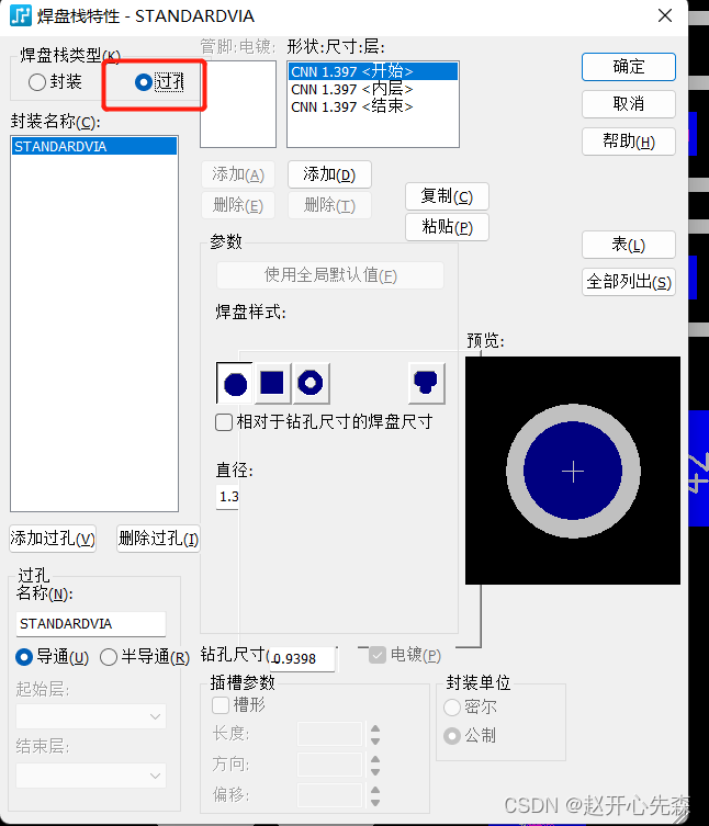
use first 1 Add via at , then 2 Set the via name at ,3 Set the via size , After that, the diameter of all three should be changed to 24
In this way, the vias are added . The drill hole size set here is 12 Mill , Then the diameter is 24
Then add design rules , First, enter the following options , Please use before setting um Set the unit to mils .
Then click the default option ,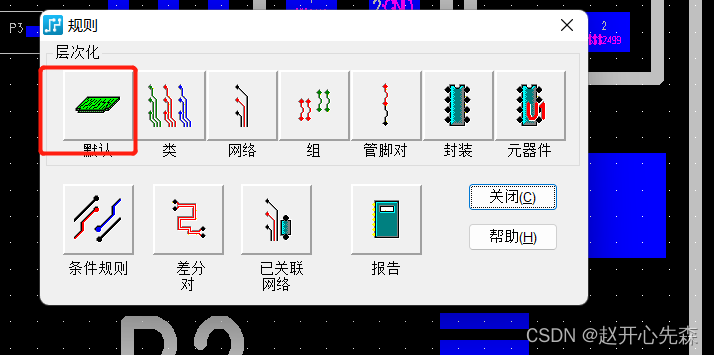
First set the safety clearance , See the following figure for options 
The following options are mainly set , Generally, it can be set as follows .
Then we set different colors for different networks , Right click the blank space to pop up the option , And then choose Select the network Options , All the same networks will be automatically selected ,
Select the network, right-click and select View network option ,
Set the following options , Then the application can 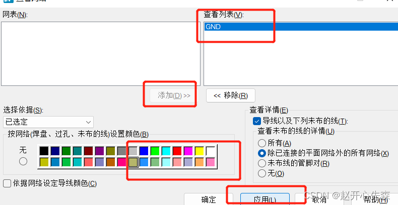
The set interface is shown in the following figure 
Then set different values for different voltage networks in turn . And then click route Start Wiring .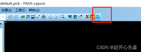
When wiring, if the wiring is very thin like this, it will affect the feeling .
You need to set the options shown in the following figure 
Then find the options shown in the figure below , Set to 0
Set the options 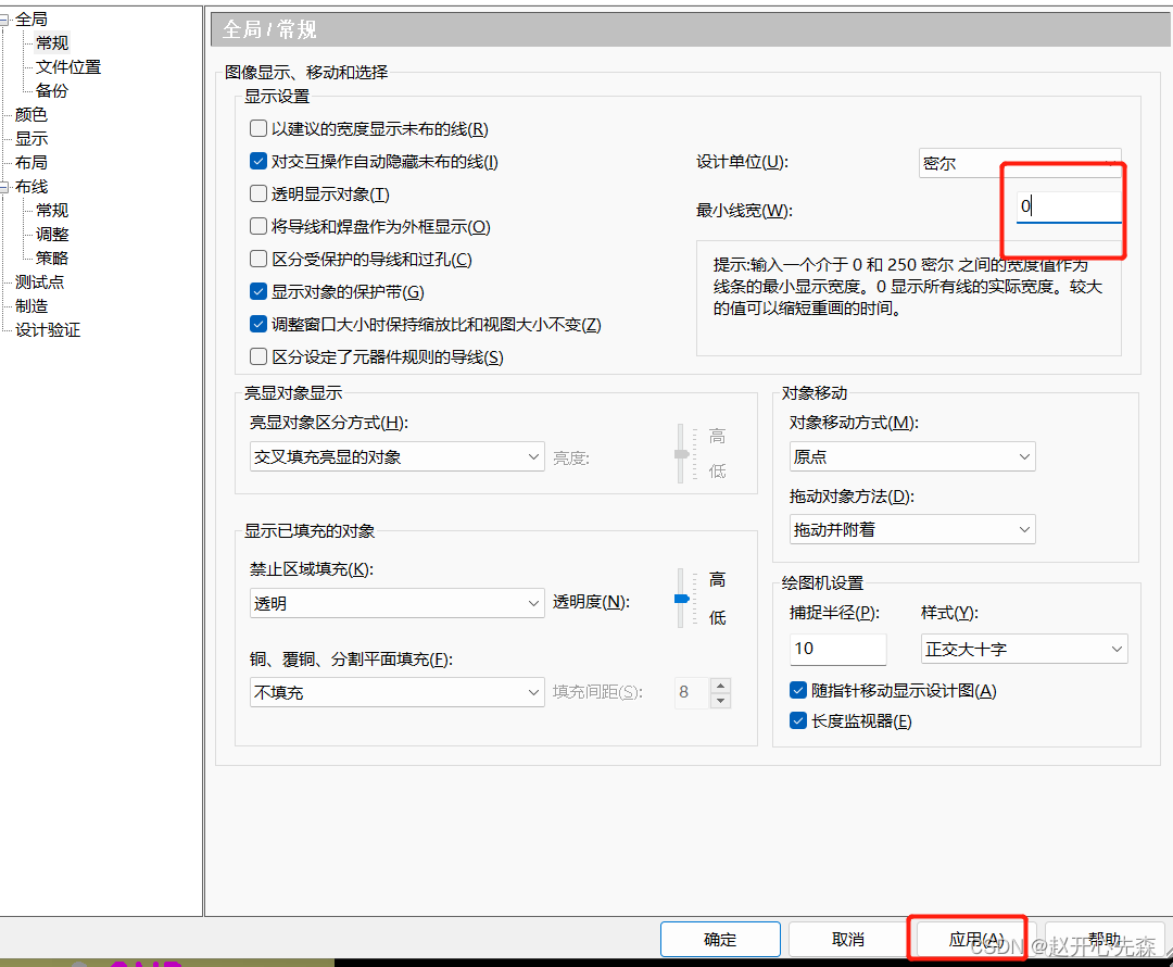
The line coming out in this way is normal .
The next step is to start wiring . Like this, you can only route on grid points , So how do we close it 
First, double-click the blank space , Then the following options appear , Select grid 
Set it as follows .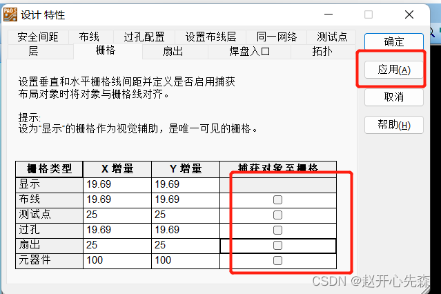
边栏推荐
- (solve) the kV store down problem of Splunk
- Redis RDB and AOF
- 12. AQS of abstractqueuedsynchronizer
- node结合art-template 模板引擎 创建模板文件
- 4K投影儀哪款性價比最高,當貝X3 Pro高亮128G存儲618值得看
- This is our golden age
- Master-slave replication of MySQL
- General O & M structure diagram
- Record a troubleshooting of MySQL master-slave asynchrony
- 美容院管理系统如何解决门店运营的三大难题?
猜你喜欢

How can physical stores break through operational difficulties? Take a look at the store operation guide of this physical store applet

MCtalk创业声音丨博学明辨:兴趣社交,给退休前后老年朋友的「小而美」空间

Splunk health checks orphaned searches
美创科技数据安全管理平台荣获2022数博会“领先科技成果奖”

Unity 游戏保护“大练兵”,一文读懂游戏事前防御

How Oracle exports data to CSV (Excel) files

Technical difficulties of secsha

11. Synchronized and lock escalation

Troubleshoot Splunk kvstore "starting"

Master-slave replication of MySQL
随机推荐
Shut down THP of Splunk health check
秒杀整体的技术难点
Troubleshoot Splunk kvstore "starting"
Serveur FTP: téléchargement et utilisation de Serv - U
(recommended) how many splunks are appropriate? Search head
Flick grouping sets multidimensional aggregation and setting table state expiration time
Flip window join, interval join, window cogroup
母婴店的利润来源有哪些?
Harmonyos application development -- mycalculator based on self-made grid layout [my calculator][api v6]
How can physical stores break through operational difficulties? Take a look at the store operation guide of this physical store applet
(solve) the kV store down problem of Splunk
Quel projecteur 4K est le meilleur rapport qualité - prix, quand bex3 pro met en évidence 128g Storage 618 vaut la peine de voir
Mctalk's entrepreneurial voice - erudition and discernment: be interested in socializing, and provide a "small and beautiful" space for old friends before and after retirement
Splunk best practices - lighten the burden on Captain
2、CompletableFuture
Master-slave replication of MySQL
CMD of Jerry's AI protocol_ SET_ BT_ Addr [chapter]
4K投影儀哪款性價比最高,當貝X3 Pro高亮128G存儲618值得看
知麻Z1投影仪真的好用吗?实际效果怎么样?
Flink physical partition (random partition, polling partition, rescaling partition, broadcast, global partition, custom partition)