当前位置:网站首页>Schematic diagram of crystal oscillator clock and PCB Design Guide
Schematic diagram of crystal oscillator clock and PCB Design Guide
2022-07-03 23:03:00 【ltqshs】
In a circuit system , The clock is an essential part . The clock circuit is quite critical , The function in the circuit is like the function of human heart , If the clock of the circuit system goes wrong , The system will be disordered , So in PCB It is very necessary to design a good clock circuit in .
Our common clock circuits are : Crystal 、 Crystal oscillator 、 Clock distributor . There are some IC The clock used may be generated by the main chip , But back to the source , It is also produced by one of the above three . Next, combined with specific examples , Explain the clock circuit layout 、 Wiring principles and precautions .
1. Crystal
PCB Commonly used crystal packages in :2 Plug in package and SMD encapsulation 、4 Pin of SMD encapsulation , Common packages are shown in the figure below :
Although the crystal has different specifications , But their basic circuit design is consistent , therefore PCB Layout 、 Wiring rules are also universal . The basic circuit design is shown in the figure below :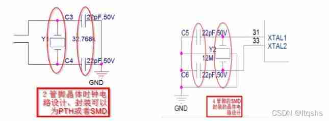
It can be seen from the circuit schematic diagram , The circuit consists of crystals +2 It consists of two capacitors , These two capacitors are gain capacitance and phase capacitance .
Crystal circuit layout , Two capacitors are placed close to the crystal , The layout rendering is as follows :
When wiring , A pair of lines in the crystal should be in the form of quasi difference , The line shall be as short as possible 、 And it should be thickened and wrapped , The effect is as follows :
The above is the most basic and common crystal circuit design , There are also some deformation designs , If adding series resistance 、 Test points, etc , Here's the picture , The design idea is consistent :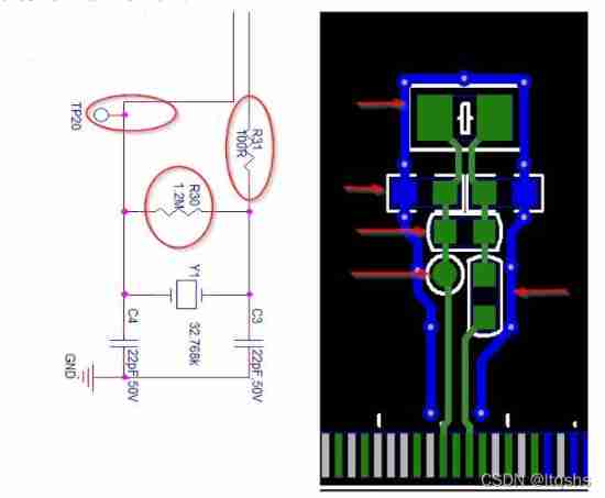
Combined with the above ,
The layout should pay attention to :
and IC Cloth on the same level , In this way, less holes can be punched ;
The layout should be compact , The capacitor is located between the crystal and IC Between , And placed close to the crystal , Make the clock line to IC Try to be as short as possible ;
For cases with test points , Try to avoid stub Or make stub Try to be as short as possible ;
Do not place high-power devices nearby 、 Such as power chip 、MOS tube 、 Inductance and other devices with high calorific value ;
Pay attention to wiring :
and IC Same floor layout , Routing on the same floor , Make as few holes as possible , If you punch , Need to add a return hole nearby ;
Class differential routing ;
The line should be bold , Usually 8~12mil; Because the crystal clock waveform is a sine wave , So here we deal with it according to the idea of simulation design ;
Signal wire package ground processing , And the shielding ground hole shall be made for the ground wire or copper sheet ;
The crystal circuit module area is equivalent to the analog area , Try not to have other signals cross ;
2. Crystal oscillator
Compared with crystal circuit , Crystal oscillator is an active circuit , It mainly consists of three parts : Crystal oscillator + Power filter circuit + Source matching resistance : The common circuit design is shown in the figure below :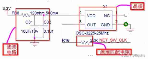
The layout and wiring effect diagram is as follows :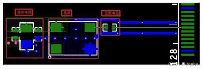
Layout 、 Wiring summary :
The filter capacitor is close to the power pin , Follow the principle of big before small , The small capacitor is closest ;
The matching resistor is placed close to the crystal oscillator ; If there is no such resistor in the schematic , It is suggested to add ;
Do not place high-power devices nearby 、 Such as power chip 、MOS tube 、 Inductance and other devices with high calorific value ;
Clock line press 50 Ohmic impedance line ; If the clock line is too long , You can walk inside , Add a reflux hole at the hole changing layer ;
Other signals remain the same as the clock signal 4W spacing ;
Parcel handling , And add shielding ground hole ;
3. Clock distributor
There are many kinds of clock distributors , In the design, ensure that the clock distributor to each IC Keep the distance as short as possible , Usually placed in a symmetrical position , for example :
Clock distributor circuit :
The design is as follows :
Layout 、 Wiring summary :
- The clock generation circuit should be close to the clock distributor , The common clock generation circuit is crystal 、 Crystal oscillator circuit ;
- The clock distribution circuit is placed in a symmetrical position , Guarantee to all IC The clock signal circuit of should be as short as possible ;
- Do not place high-power devices nearby 、 Such as power chip 、 MOS tube 、 Inductance and other devices with high calorific value ;
- When the clock signal line is too long , You can walk inside , Change the layer hole 200mil There should be a backflow through hole in the range ;
The above content comes from official account “ Big talk hardware ” 《 Reference to the original :PCB Modular layout — Clock circuit design 》
边栏推荐
- How to solve the problem of requiring a password when accessing your network neighborhood on your computer
- The difference between SRAM and DRAM
- Data consistency between redis and database
- 4 environment construction -standalone ha
- [issue 16] golang's one-year experience in developing Purdue Technology
- ADB related commands
- In VS_ In 2019, scanf and other functions are used to prompt the error of unsafe functions
- 320. Energy Necklace (ring, interval DP)
- Ansible common usage scenarios
- Hcip day 15 notes
猜你喜欢

In 2022, 6G development has indeed warmed up

Scratch uses runner Py run or debug crawler
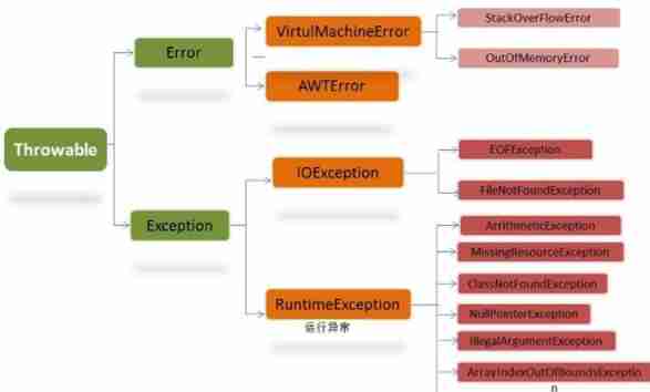
Summary of basic knowledge of exception handling

Team collaborative combat penetration tool CS artifact cobalt strike

Summary of fluent systemchrome
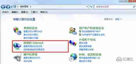
How to solve the problem of requiring a password when accessing your network neighborhood on your computer

Qtoolbutton - menu and popup mode

Weekly leetcode - nc9/nc56/nc89/nc126/nc69/nc120
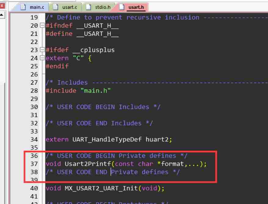
STM32 multi serial port implementation of printf -- Based on cubemx

Cesium terrain clipping draw polygon clipping
随机推荐
Is the controller a single instance or multiple instances? How to ensure the safety of concurrency
Programming language (1)
C3p0 connection MySQL 8.0.11 configuration problem
Leetcode: a single element in an ordered array
Codeforces Round #768 (Div. 1)(A-C)
Unity shader visualizer shader graph
Qtoolbutton - menu and popup mode
Plug - in Oil Monkey
33 restrict the input of qlineedit control (verifier)
In 2022, 6G development has indeed warmed up
X Opencv feature point detection and matching
LeetCode 1647. Minimum deletion times of unique character frequency
Teach you how to run two or more MySQL databases at the same time in one system
Interesting 10 CMD commands
Niuke winter vacation training camp 4 g (enumeration optimization, Euler power reduction)
Ten minutes will take you in-depth understanding of multithreading. Multithreading on lock optimization (I)
Summary of basic knowledge of exception handling
[golang] leetcode intermediate - alphabetic combination of island number and phone number
JS closure knowledge points essence
Quick one click batch adding video text watermark and modifying video size simple tutorial