当前位置:网站首页>EMC design scheme of CAN bus
EMC design scheme of CAN bus
2022-07-27 15:16:00 【Desert fall】
One . CAN Interface EMC Design Overview
Controller Area Network Referred to as CAN, It is mostly used in automobile and industrial control , For data transmission control . In the process of application, the communication cable is easy to be coupled with external interference, which will have a certain impact on signal transmission , The interference inside the board may also form external radiation through the cable .
This scheme starts from EMC On the principle of , Schematic diagram of the interface 、PCB、 The structure and cable shall be designed for interference suppression and anti sensitivity , Solve from the design level EMC problem .
This scheme can pass the automotive electronic standard CISPR 25-2008 And ISO7637 Series standard , Or you can pass the following test items :
Serial number | Interface test items | Test level | Performance criterion |
1 | Radiation emission (RE) | CISPR25 LV5 | |
2 | Conducted emission (CE) | CISPR25 LV5 | |
3 | RF magnetic field immunity (RI) | 400~4000MHz 150V/m Dwell time 2s | Performance criterion A |
4 | High current injection BCI | 1~400MHz 150mA 150mm Dwell time 2s | Performance criterion A |
5 | Conducted immunity 7637-2 (24V System ) | wave form 1:Us=-450V 10000 pulses wave form 2a:Us=+50V 10000 pulses wave form 2b:Us=+20V 20 pulses wave form 2a:Us=-150V 1h wave form 3b:Us=+150V 1h wave form 5b:Us=-+30V Td=250ms | Performance criterion C Performance criterion A Performance criterion C Performance criterion A Performance criterion A Performance criterion A |
6 | Electrostatic immunity ESD | Contact :+-8KV air :+-15KV | Performance criterion A |
Two . Schematic design scheme
1. CAN Interface anti-static design
chart 1 CAN Interface anti-static design
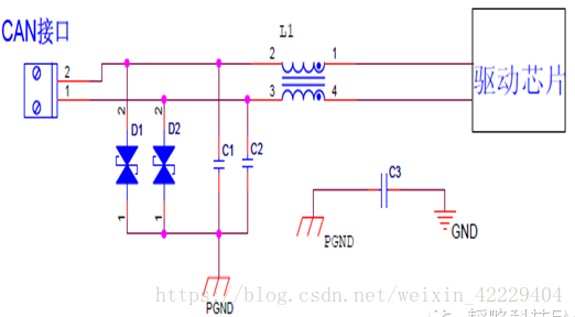
circuit EMC Design description :
(1) Key points of circuit filter design :
L1 For common mode inductance , It is used to filter the common mode interference on the differential line , The impedance selection range is 120Ω/100MHz ~2200Ω/100MHz, Typical value selection 600Ω/100MHz;
C1、C2 Is the filter capacitance on the signal line , Provide a low impedance return path for interference , The selection range of capacitance value is 22PF~1000pF, Typical value selection 100pF;
C3 It is the jumper capacitance between interface ground and digital ground , The typical value is 1000pF, The withstand voltage shall meet the requirements of 2KV above ,C3 The capacitance value can be adjusted according to the test situation ;
(2) Key points of circuit protection design :
D1、D2 It is a transient suppression diode , Typical selection requires reverse shutdown voltage 3.5V above ; because TVS Just for electrostatic protection ,TVS The power is not required .TVS The junction capacitance of the transistor has a certain influence on the signal transmission ,CAN It is recommended that the junction capacitance be less than 100pF Of TVS tube .
Interface circuit design remarks :
If the equipment is metal enclosure , At the same time, the board can be divided into interfaces independently , Then the metal shell is directly electrically connected with the interface ground , And the single board and the interface pass through 1000pF Capacitors are connected ; If the equipment is non-metallic shell , So the interface PGND And veneer ground GND Direct electrical connection .
3、 ... and . PCB design scheme
1. CAN Interface division design

chart 2 CAN Interface division design
Program features :
(1) In order to suppress the high-frequency noise of the internal board, the radiation is transmitted to the outside through the interface , In order to enhance the anti-interference ability of the single board to external interference . stay CAN Protective and filter isolation devices shall be added at the interface , It is bounded by the position and size of the isolation device , Divide the interface ground ;
(2) The capacitance can be selectively increased in the isolation band as the connection between the two ground , The recommended value of capacitance is 1000pF; Signal line series common mode inductance filtering , And the common mode inductance is required to be placed in the isolation band ; In order to prevent strong external interference, it is coupled into the interior through the port PCB, Cause performance degradation of internal devices , Add protective devices on the signal line near the port TVS tube , The specific layout is shown in the figure .
Scheme analysis :
(1) When there are circuits with poor compatibility or incompatibility between the interface and the board , The interface needs to be connected with the board “ Division of land ” Handle , That is, according to different port voltages 、 Set the ground wire according to the signal level and transmission rate .“ Division of land ”, It can prevent the superposition of return signals of incompatible circuits , Prevent impedance coupling of common ground wire ;
(2) CAN The interface signal transmission rate is high , Inside PCB The high-frequency noise of the board is easily transmitted and radiated from the common ground through the interface , Therefore, the common ground is divided and connected through capacitance , It can block the propagation path of common mode interference .
2. CAN Interface circuit layout

chart 3 CAN Interface filtering and protection circuit layout
Program features :
(1) Protective devices and filter devices shall be placed close to the interface and shall be placed compactly and neatly , Protective devices on signal lines TVS The tube and filter capacitor shall be connected to the interface ground ; Place the device according to the signal flow direction , When routing, try to avoid routing twists and turns ;
(2) Common mode inductance and jumper capacitance shall be placed in the isolation band .
Scheme analysis :
(1) The interface and interface filter protection circuit shall not be wired and high-speed or sensitive devices shall not be placed around ;
(2) The projection layer below the isolation belt shall be hollowed out , No routing .
Four . Structural design scheme
1. CAN Signal connector pin definition

chart 4 CAN Signal connector
Connector signal pin definition
(1) If it is a single group CAN The signal , Then select two adjacent pins as the differential signal ;
(2) If multiple groups CAN The signal is in the same connector , Then a ground pin should be defined between each group of signals to isolate each other . As shown in the figure above :
5、 ... and . Cable design scheme
1. CAN Signal cable assembly

chart 5 CAN Signal cable assembly
Cable design :
(1) CAN The signal cable adopts the shielding method of mesh braided shielding layer , And the braiding density of the mesh braid shall not be less than 90%;
(2) When assembling lines inside , The differential cable adopts twisted pair transmission , The twisted pair pitch is generally 3 times ; The wiring method is shown in the above figure :
(3) Magnetic rings need to be added at both ends of the cable , The inner diameter of the magnetic ring should be closely combined with the outer diameter of the cable , Try to choose thick and long magnetic rings .
Wiring design :
(1) CAN The signal cable shall be far away from other strong interference sources , Such as power module ;
(2) It is better to route the cable separately or keep it with other analog and power cables 250px The distance above , Do not mix and bind with other cables .
EDP The software is introduced
EMC design platform (EDP) , According to the most professional EMC Expert program knowledge base , Quickly output the guidance that meets the requirements of product design EMC Solution .
Main function modules :

EDP Software workflow

边栏推荐
- 仅做两项修改,苹果就让StyleGANv2获得了3D生成能力
- JUC(JMM、Volatile)
- 反射
- Notice on printing and distributing the Interim Measures for the administration of green manufacturing pilot demonstration of Shenzhen Bureau of industry and information technology
- STM32 can -- can ID filter analysis
- 对话框管理器第三章:创建控件
- 网络设备硬核技术内幕 路由器篇 (10) CISCO ASR9900拆解 (四)
- 魔塔项目中的问题解决
- 网络设备硬核技术内幕 路由器篇 14 从鹿由器到路由器 (中)
- reflex
猜你喜欢

适配验证新职业来了!华云数据参与国家《信息系统适配验证师国家职业技能标准》编制

反射

USB2.0接口的EMC设计方案

JMeter recording interface automation

STM32F103C8T6在Arduino框架下驱动SH1106 1.3“ IIC OLED显示

3.3-5v conversion
移动端使用vantUI的list组件,多个tab项来回切换时,列表加载多次导致数据无法正常展示

Getting started with DirectX

Design scheme of digital oscilloscope based on stm32

Unity performance optimization ----- LOD (level of detail) of rendering optimization (GPU)
随机推荐
关于 CMS 垃圾回收器,你真的懂了吗?
Unity性能优化------渲染优化(GPU)之Occlusion culling(遮挡剔除)
【云享读书会第13期】多媒体处理工具 FFmpeg 工具集
Kotlin的基础用法
《剑指Offer》剪绳子
网络设备硬核技术内幕 路由器篇 11 CISCO ASR9900拆解 (五)
网络设备硬核技术内幕 路由器篇 18 DPDK及其前传(三)
MOS管防止电源反接的原理
光电隔离电路设计方案(六款基于光耦、AD210AN的光电隔离电路图)
Usage of countdownlatch in multithreaded environment
Nefu117 number of prime numbers [prime number theorem]
《剑指Offer》两个链表的第一个公共结点
Design scheme of digital oscilloscope based on stm32
Kubernetes CNI classification / operation mechanism
The mobile terminal uses the list component of vantui. When multiple tab items are switched back and forth, the list is loaded many times, resulting in the failure of normal display of data
网络设备硬核技术内幕 路由器篇 9 CISCO ASR9900拆解 (二)
DXGI acquisition process
Unity performance optimization ----- occlusion culling of rendering optimization (GPU)
Sword finger offer cut rope
移动端使用vantUI的list组件,多个tab项来回切换时,列表加载多次导致数据无法正常展示