当前位置:网站首页>FPGA timing constraint sharing 01_ Brief description of the four steps
FPGA timing constraint sharing 01_ Brief description of the four steps
2022-07-04 19:30:00 【MDYFPGA】
This article is an original article by Ming Deyang , Reprint please indicate the source !
This article discusses FPGA Timing constraint steps , The content of this article , It comes from the configured video of mingdeyang timing constraint special course .
Timing constraint is a very important content , And there are many contents , Relatively miscellaneous . therefore , Many readers have questions about how to constrain , The steps and processes of constraints, etc , Not very clear . Ming Deyang, based on the experience of previous projects , The steps of timing constraints , The summary is divided into four big steps , They are the constraints of the clock 、input delays Constraints 、output delays Constraints and timing exceptions .
Timing constraints are sequential , First of all, we need to make clock constraints 、 The second is input delays constraint 、 Again output delays constraint , Finally, the constraints of timing exceptions . This is a complete big step , In other words, we can restrict our clock at the beginning of the project , Put the frequency of our clock 、 cycle 、 Source, etc. well defined . When this is done , Don't do two, three or four steps first . At this time, we have to finish our design , We need to complete our internal timing before setting the second step “input delays”, For example, when we came in from the outside . The third step output delays, That is to say, a timing situation to be sent to downstream devices . When this one, two or three steps are completed , We only made a timing exception in the final stage of the project . Time series exceptions, that is, which time series do not need to be analyzed , This situation should be set well . Finally, we can complete the whole timing constraint .
These are big steps , But in fact, each step can be subdivided into many situations . For example, clock constraints , Clocks can be divided into many kinds , One is differential clock , One is the clock with the pin coming in 、 And we PLL Generate clock and so on . There is also a case where there is data but no clock .input delays、output delays There are many kinds , How do we analyze , How to see . Ming Deyang refined these four steps , It is to list them separately according to the situation .

The following is a description .
The first 1 section The clock
Clock constraints can be divided into many situations , Different cases have different constraint methods , What are the general situations ?
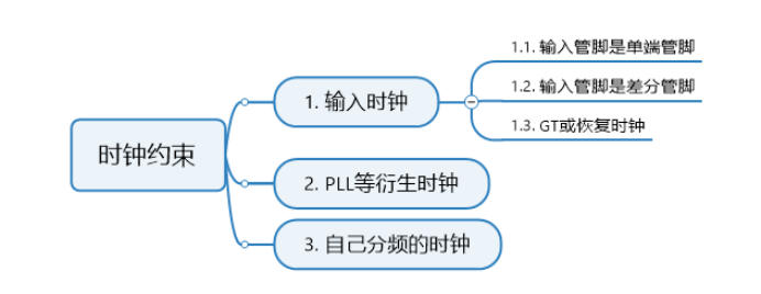
Pictured above , Clock constraints can be summarized as , It can be divided into three situations , They are the input clock 、PLL And other derivative clocks and their own step-by-step clocks .
1.1 Input clock
The input clock refers to the clock from FPGA When the pin comes in , This is also the most common situation . According to the input pins , The input clock can be divided into : The input pin is single ended 、 The input pin is differential , as well as GT Or restore the clock .
The first one is : The input pin is single ended , The real-time clock comes in directly from the pin 、 And it's a single ended signal . For example, ordinary low-speed crystal oscillator , This is mostly the case , Mingdeyang's FPGA ALTERA Learning board , Such as MP801、MP603, The clock is produced by crystal oscillator , Deliver to FPGA, And it's a single ended signal .
The second kind : The input pin is differential , The real-time clock comes in directly from the pin , And it's a differential signal . Most high-speed crystal oscillators 、LVDS Interfaces, etc. , In this case . For example, Ming Deyang FPGA XILINX Learning board , Such as MP802, It contains PCIE Pin , The input clock is differential ; This board is DDR The drive clock of , The clock frequency is at 200M about , This is also the case .
The third kind of :GT Or restore the clock , That is, when a high-speed transceiver is used . In the high-speed transceiver pin , There is no clock , The clock has been embedded in the data , Use FPGA Of GTX IP Nuclear receive data , And recover the clock from the data . This is the case with the recovered clock . The most common is the optical fiber interface .
1.2 PLL And so on
If I'm not an input pin , It is PLL Generated output clock , This Namely PLL And so on . This kind of clock ,FPGA Tools for , I'll deduce it myself , Generally, there is no need to restrict , But in practical application , It is strongly recommended to restrict , It's going to be good , The benefits are explained in the next article .
1.3 Own frequency division clock
There is also a case of its own frequency division clock , Let's say we wrote a counter ourselves , Divide it in two 、 Quad frequency 、 Eight frequency division, etc , The divided signal is used as a clock , This situation is the clock of its own frequency division .
First of all , Mingdeyang does not recommend using this method to generate clock . But when you do need a frequency division clock , Then remember to make clock constraints . How to constrain in this case ?
The above summarizes several situations of the clock , In each case , The constraint methods are somewhat different and the points for attention . Specific constraint methods , You can see the contents of the following articles .
The first 2 section input delays
input delay constraint , Input delay constraint , Timing constraints are important ,input delay There are several kinds ?

Pictured above ,input delay Constraints generally , It can be divided into three situations , System synchronization 、 Source synchronization and data without clock .
2.1 System synchronization
The first is the system synchronization mode , That is to say, on the whole circuit board FPGA And upstream devices share a clock , And the phase is strictly the same , This is the way of system synchronization .
2.2 Source synchronization
The second is source synchronization , How is source synchronization ? Upstream devices , Send the data together with the clock signal FPGA Coming up , This is source synchronization .
Source synchronization is a more common method , System synchronization is less used , Why? ? Because the upstream devices should follow FPGA The phase difference is 0, There's no clock difference , This requirement is very high . And source synchronization is that data and clock are transmitted from upstream devices to FPGA, This is a more common way .
This source is synchronized , There are many kinds , Specifically SDR、DDR And with data and without clock .
The first one is :SDR.SDR It means that the clock is a single edge effective way , For example, I only use the way of rising or falling ,SDR Parameters of constraints , There are two ways to obtain it : Check the upstream device manual ( By checking the data book of the upstream device , To obtain parameters ) And measured by oscilloscope ( Measure the phase difference of the signal through an oscilloscope , To obtain parameters ).
The second kind :DDR.DDR It's another way , It is an effective way of clock double edge . That is to say, use its rising extension , Also use its descent delay . For example, our DDR2、DDR3 The clock of , All data are collected from the upper falling edge ; Including Gigabit Network RGMII Interface , It is also through the way of double edge .
DDR In this case , We can also continue to divide into two cases: center alignment and edge alignment .
Center alignment refers to : The edge of the clock is always in the middle of the data , The left and right sides of the rising edge of the clock , The data are stable . Edge alignment refers to : Clock and data edge aligned , On both sides of the clock , The data is unstable .
The third kind of : There is data but no clock . The third is the case of data without clock . For example, the common serial port . The serial port is used to directly transmit data , It didn't come with the clock . And we use the local clock to sample , There will be data without clock . How should we restrict this kind of , Another situation .
The first 3 section output delays
The output delay constraint is the same as the input delay , It is also the focus of constraints .output delay We mainly divide into two kinds , System synchronization and source synchronization .
3.1 System synchronization
On the whole circuit board FPGA And downstream devices share a clock , And the phase is strictly the same , This is the way of system synchronization . here FPGA Send data to downstream devices , At this time, only the data line can be transmitted . And the clock follows FPGA Sharing one , No need to pass the clock .
3.2 Source synchronization
Source synchronization is FPGA Send data to this device , In the process of sending data, a clock is also sent , This is a way of a random clock , It's source synchronization .
We also divide the source synchronization into SDR and DDR.
The first one is :SDR.SDR It means that the clock is a single edge effective way , For example, I only use the way of rising or falling ,SDR Parameters of constraints , There are two ways to obtain it : Check the upstream device manual ( By checking the data book of the upstream device , To obtain parameters ) And measured by oscilloscope ( Measure the phase difference of the signal through an oscilloscope , To obtain parameters ). Oscilloscope measurement is less used .
The second kind :DDR.DDR It's another way , It is an effective way of clock double edge . That is to say, use its rising extension , Also use its descent delay . For example, our DDR2、DDR3 The clock of , All data are collected from the upper falling edge ; Including Gigabit Network RGMII Interface , It is also through the way of double edge .
DDR In this case , We can also continue to divide into two cases: center alignment and edge alignment .
Center alignment refers to : The edge of the clock is always in the middle of the data , The left and right sides of the rising edge of the clock , The data are stable . Edge alignment refers to : Clock and data edge aligned , On both sides of the clock , The data is unstable .
The first 4 section Timing exceptions
Timing exceptions are generally used in clock And IO After all constraints , Or when the timing requirements are not met . It mainly includes multi periodic paths 、 There are three situations such as path and combinational circuit delay that do not need to be checked , Here's the picture .
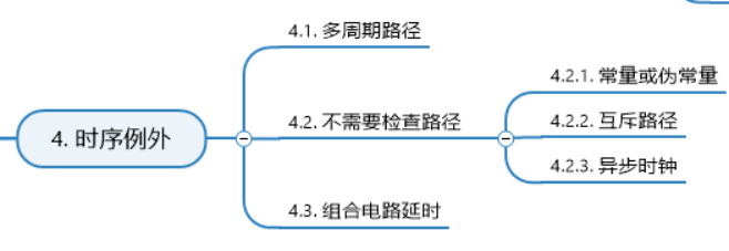
4.1 Multicycle path
Multi period path means that it takes more than... To complete an operation 1 In the case of two clock cycles , Multi periodic path in IC It is widely used in the field of design , But in FPGA Less used in .
4.2 Paths that do not need to be checked
There are some paths that do not need to be analyzed , It can be divided into three types : Constant or pseudo constant signal 、 Mutually exclusive path and asynchronous clock .
The first one is : Constant or pseudo constant signal . Although some signals do not meet the timing requirements , But in essence, the signal is in the application scenario , It won't change , For example, a switch signal , Turn it on when it's powered on , Just keep it open , It won't change around . Then this signal can be regarded as a pseudo constant signal . Suppose it does not meet the timing requirements , It doesn't matter , Because it won't change , No change means that the establishment time and holding time must be satisfied , So there's no problem . This signal does not need to be checked Of .
The second kind : Mutually exclusive paths . It can be simply considered as a two-way port , In the code , Use inout Defined signals .
The third kind of : Asynchronous clock . That is, the signal from a clock domain , Cross to another clock domain . This also does not need to be checked Of . Be careful , There is no need to check , It refers to the synchronization of asynchronous signals , Don't check means .
4.3 Combinational circuit delay
Another is the delay of combinational circuit . The delay of combinational circuit means that I go from one pin to another , The other pin comes in , There is no clock in the middle of this pin , This is a case where the combinational circuit gives time delay .
The first 5 section Summary and suggestions
We talked about clock constraints earlier 、 Input delay 、 The output delay is also an exception to timing . Each situation is divided into many kinds , Distinguish according to its different types , Each constraint is one of these situations . for instance CLK Difference , Just find the clock , Then according to the difference, how to restrict the feet , To find the corresponding situation , Constrain as required . This is equivalent to I have provided you with a table , You check according to this table . Find the corresponding situation , Just constrain as required .
remember : At the beginning , Just configure the clock , Not configured input delay 、 output delays And persistent exceptions . Because we started by focusing on the internal circuit , A design of our timing , After meeting the internal requirements , Then configure our interface . Configure after the clock passes completely input delay and output delays .
The timing exception is to configure after almost completion . And this configuration should be very careful . Because we are actually exceptional , For example, don't check , We set false path This situation , If it is set, it means that there is no need to check . If at the beginning , It's set up , In case of another change in the middle , If you change , Then you forgot to kill this constraint , In this case, there will be errors that cannot be prompted . So the timing exception should be made in the last case .
This order is an order of mingdeyang's experience , Our projects are basically done in this order . But different companies will do different things . For example, I didn't restrict myself at first , To the last regeneration constraint , That's ok . There is no uniform standard for this practice , Anyway, take mingdeyang's course , Just follow this step , Go to other companies , It's OK to do it according to the company's requirements .
This article is based on a timing constraint of Xilinx ,ALTERA It's similar , even to the extent that IC Chip design , The same idea .
There is a good saying , Our timing is designed , It's not constrained . So timing is important or not ? Of course important. . But it's not very important , More importantly, if I have an exception , When I'm not satisfied , More importantly, change your design , Instead of requiring constraints .
Next article , We will discuss in detail “ Clock constraint ” The content of , Explain the timing constraint methods in various cases . Need more and more detailed information and original documents , You can find the author to understand and receive .
Ming Deyang (MDY) In addition to training courses , It can also provide customers with projects 、FPGA chip 、 Power supply chip 、AD Chips and other components , But let us know .18922344178( Phone and wechat synchronization )
边栏推荐
- Using FTP
- Lex and yacc based lexical analyzer + parser
- Don't just learn Oracle and MySQL!
- Technology sharing | interface testing value and system
- Oracle with as ORA-00903: invalid table name 多表报错
- Li Chi's work and life summary in June 2022
- There are multiple divs in the large div, which are displayed on the same line. After overflow, scroll bars are generated without line breaks
- Rookie post station management system based on C language
- Unity editor extends C to traverse all pictures in folders and subdirectories
- QT realizes interface sliding switching effect
猜你喜欢
随机推荐
OpenCV的二值化处理函数threshold()详解
页面元素垂直水平居中、实现已知或者未知宽度的垂直水平居中。
Technologie de base de la programmation Shell IV
YOLOv5s-ShuffleNetV2
《工作、消费主义和新穷人》的微信读书笔记
The difference and usage between substr (), slice (), and substring () in the string interception methods of "understand series after reading"
876. 链表的中间结点
26. Delete the duplicate item C solution in the ordered array
Unity编辑器扩展C#遍历文件夹以及子目录下的所有图片
[uniapp] uniapp development app online Preview PDF file
使用SSH
偏移量函数及开窗函数
Go microservice (II) - detailed introduction to protobuf
6.26cf simulation race e: solution to the problem of price maximization
Using FTP
基于NCF的多模块协同实例
Build your own website (15)
The 300th weekly match of leetcode (20220703)
Shell 编程核心技术《四》
在线SQL转Excel(xls/xlsx)工具


