当前位置:网站首页>Semiconductor devices (I) PN junction
Semiconductor devices (I) PN junction
2022-07-05 08:01:00 【Drink more hot water-】
( One ) Intrinsic semiconductor Impurity semiconductor
Intrinsic semiconductor It is a semiconductor with pure crystal structure . The impurities 、 Have a stable structure .
At a certain temperature, the carrier concentration in the intrinsic semiconductor is certain , And the concentration of free electrons and holes is equal .
Impurity semiconductor There are two kinds of :N Type semiconductor P Type semiconductor
N Type semiconductor :
Intrinsic semiconductor doping 5 After the valence element , Some silicon atoms in the original crystal will be replaced by impurity atoms . The outermost layer of impurity atoms has 5 A valence electron , among 4 A covalent bond with silicon , More than one electron is attracted only by its own nucleus , It can become a free electron at room temperature .
Electrons are called majority carriers ( abbreviation children ),Negitive
Holes are called minority carriers ( abbreviation Young son ).
5 Valence impurity atoms are called Donor atom .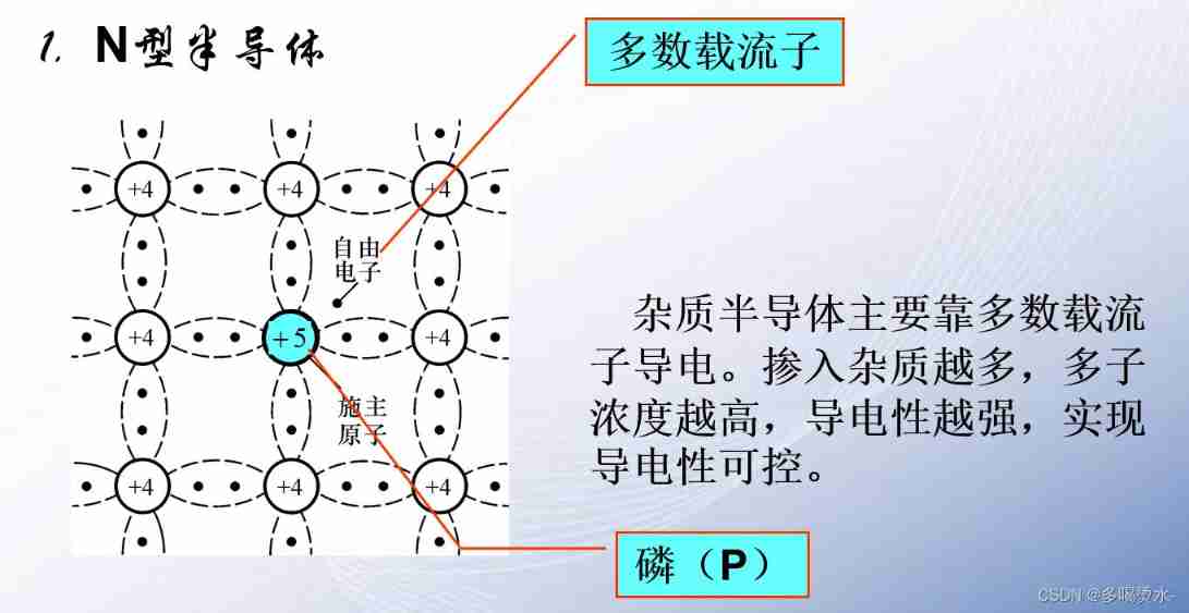
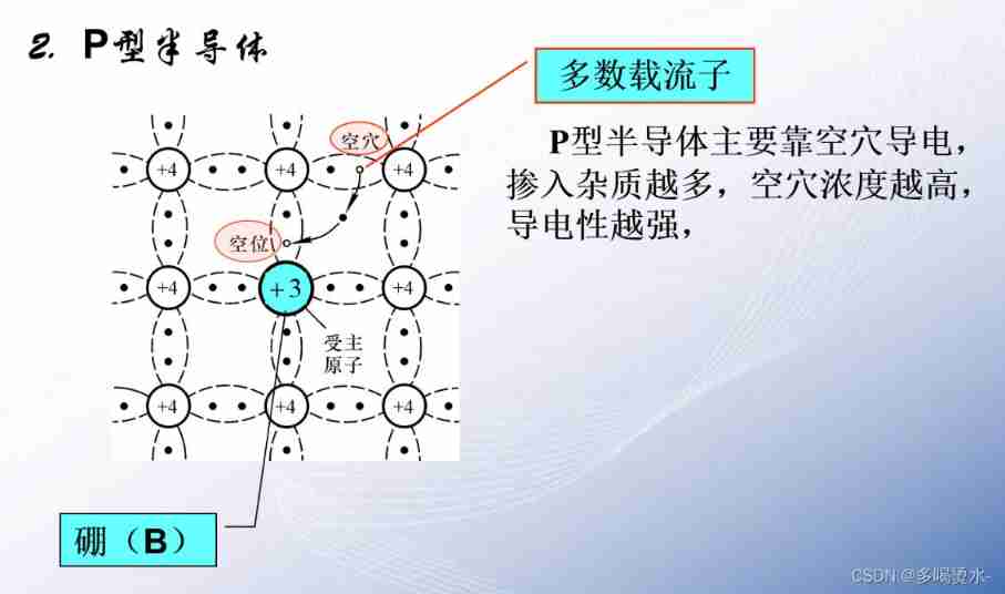
P Type semiconductor
In silicon or germanium crystal doped with a small amount of 3 Valence impurity element , Like boron 、 gallium 、 Indium, etc , Composition P Type semiconductor .The hole is ** Most carriers **,Positive Electron is ** Minority carriers ** 3 Valence impurity atoms are called ** Acceptor atom **.
explain :
1. The concentration of doped impurities determines the concentration of most carriers ; Temperature determines the concentration of minority carriers .
2. The number of carriers in impurity semiconductors is much higher than that of intrinsic semiconductors , Therefore, its conductivity is greatly improved .
3. Impurity semiconductors generally remain electrically neutral .
( Two ) PN The formation of knots
PN junction Formation process : Spread 、 Drift movement
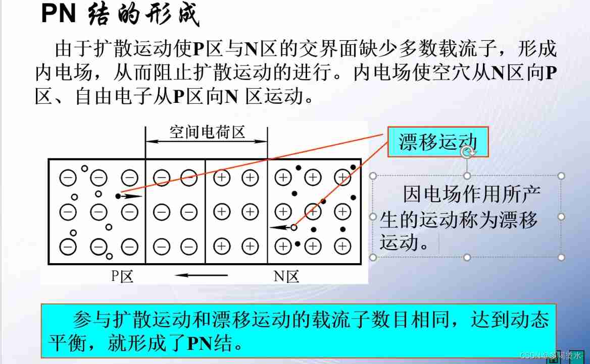
Doping on one side of a semiconductor single crystal becomes P Type semiconductor , The other side is doped into N Type semiconductor , A special thin layer is formed at the junction of the two areas , be called PN junction .
original P Area and N All areas are electrically neutral , because children The spread of , It will inevitably lead to the destruction of the electrical neutrality inside the semiconductor , Thus in the conductor PN An internal electric field is formed at the junction : Pay attention to the direction of the internal electric field 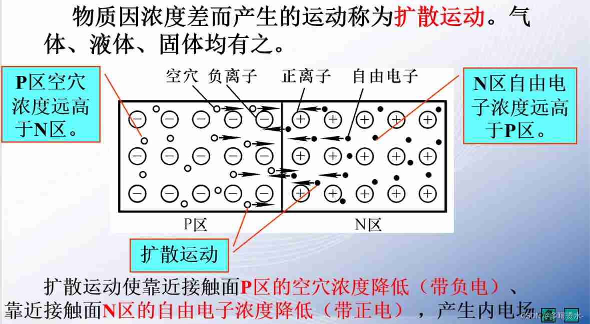
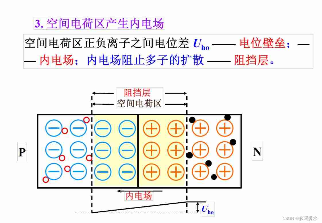
The width of the depletion layer is determined by the intensity of the diffusion movement . The resistivity of the depletion layer is very high , It is high resistance area . This is because the resistance reflects the conductivity , The depletion layer has reached dynamic equilibrium , Basically non-conductive , Natural resistance is very large .
Although whether it is diffusion motion or drift motion , The actual motion is all electrons . But in order to distinguish between diffusion motion and drift motion , Diffusion motion is often referred to as multiparticle motion , Because diffusion is the process of many children in this region entering the other region ; The corresponding drift motion becomes the minority carrier motion .
( 3、 ... and )PN The nature of the knot
3.1 Unidirectional conductivity 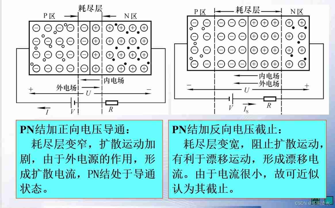
stay PN Add a small forward voltage to the junction , You can get a larger forward current , To prevent excessive current , Resistance can be connected R.
Reverse current is also called reverse saturation current I S. Very sensitive to temperature , As the temperature rises , IS Will increase dramatically .
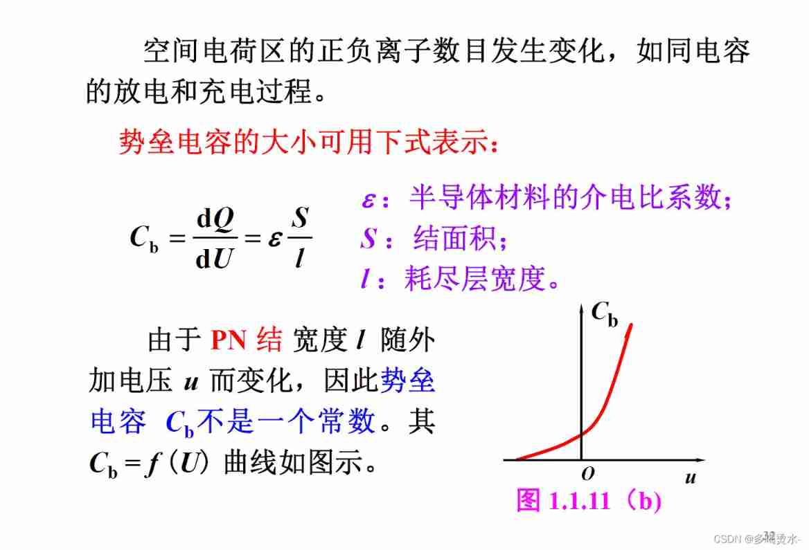
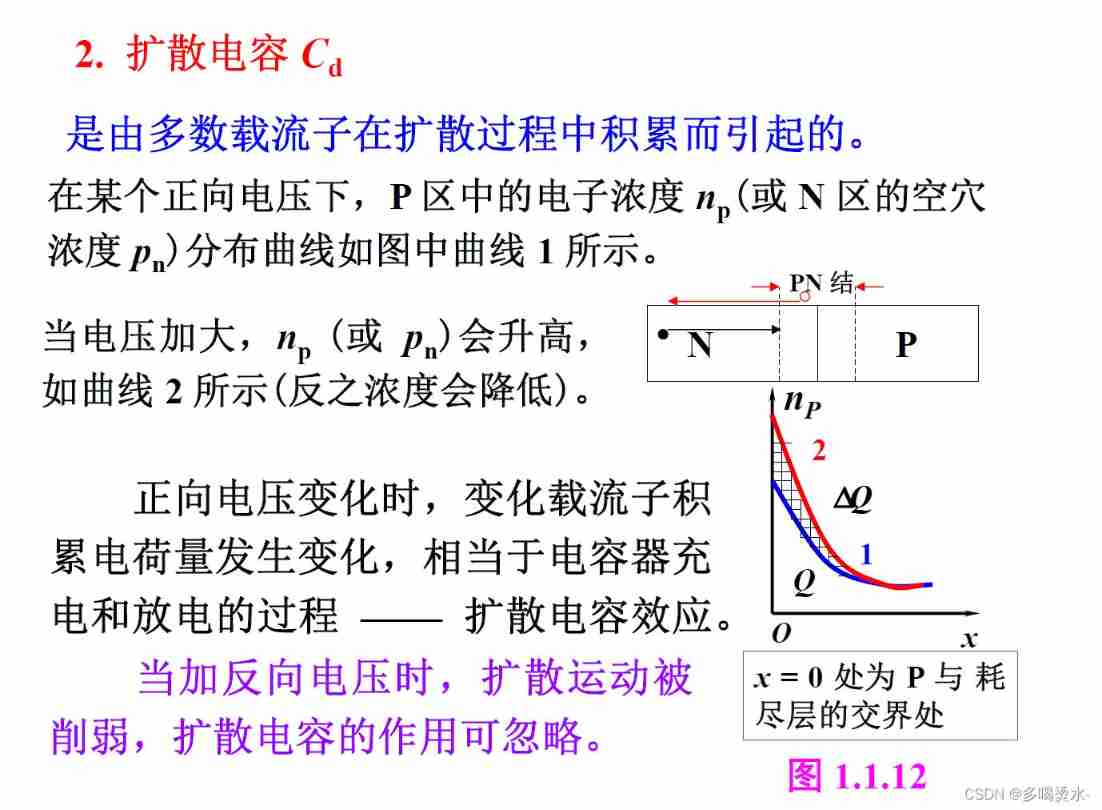
3.2 PN The capacitance effect of the junction
When PN When the voltage on the changes ,PN The amount of charge stored in the junction will change accordingly , send PN The junction has a capacitive effect .
Capacitance effect includes two parts : Barrier capacitance 、 Diffusion capacitance 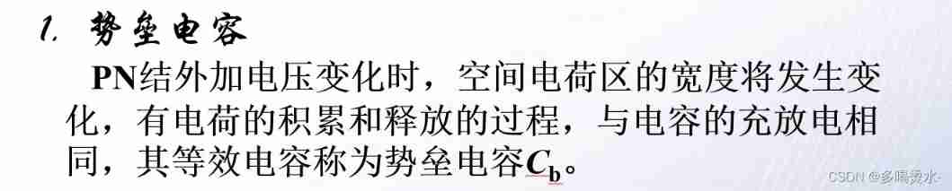

边栏推荐
- Factors affecting the quality of slip rings in production
- 研究發現,跨境電商客服系統都有這五點功能!
- Global and Chinese market of quenching furnaces 2022-2028: Research Report on technology, participants, trends, market size and share
- Altium designer 19.1.18 - change the transparency of copper laying
- Global and Chinese market of peeled bourdon tubes 2022-2028: Research Report on technology, participants, trends, market size and share
- 1-stm32 operation environment construction
- The firmware of the connected j-link does not support the following memory access
- The research found that the cross-border e-commerce customer service system has these five functions!
- Realization of binary relation of discrete mathematics with C language and its properties
- Basic embedded concepts
猜你喜欢
![Halcon's practice based on shape template matching [2]](/img/70/3e905661785e570fb406b8e97d41e6.jpg)
Halcon's practice based on shape template matching [2]
![C WinForm [view status bar -- statusstrip] - Practice 2](/img/40/63065e6c4dc4e9fcb3e898981f518a.jpg)
C WinForm [view status bar -- statusstrip] - Practice 2

The research found that the cross-border e-commerce customer service system has these five functions!
Relationship between line voltage and phase voltage, line current and phase current
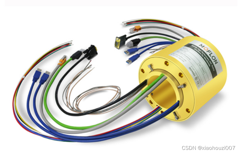
生产中影响滑环质量的因素
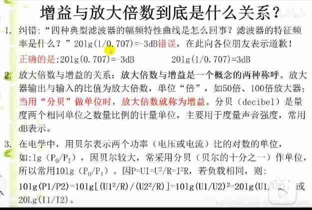
Hardware 1 -- relationship between gain and magnification
![Measurement fitting based on Halcon learning [II] meaure_ pin. Hdev routine](/img/da/8c70699d2cd3ec5b36ec716b8f6bd1.jpg)
Measurement fitting based on Halcon learning [II] meaure_ pin. Hdev routine
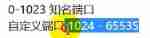
Network port usage
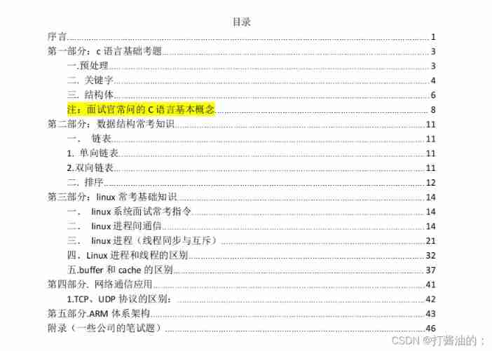
Interview catalogue
How to select conductive slip ring
随机推荐
Altium designer 19.1.18 - change the transparency of copper laying
Class of color image processing based on Halcon learning_ ndim_ norm. hdev
C, Numerical Recipes in C, solution of linear algebraic equations, LU decomposition source program
The printer encountered an abnormal configuration problem 0x8007007e (win10)
[untitled] record the visual shock of the Winter Olympics and the introduction of the display screen
Extended application of single chip microcomputer-06 independent key
Global and Chinese market for blood typing 2022-2028: Research Report on technology, participants, trends, market size and share
Shell script basic syntax
Network communication model -- Network OSI tcp/ip layering
Summary -st2.0 Hall angle estimation
Makefile application
Distinction between heap and stack
Shape template matching based on Halcon learning [v] find_ cocoa_ packages_ max_ deformation. Hdev routine
研究发现,跨境电商客服系统都有这五点功能!
UEFI development learning 6 - creation of protocol
Reasons for rapid wear of conductive slip rings
UEFI development learning series
How to select conductive slip ring
Hardware 3 -- function of voltage follower
UEFI development learning 5 - simple use of protocol