当前位置:网站首页>Digital integrated circuit: MOS tube device chapter (I)
Digital integrated circuit: MOS tube device chapter (I)
2022-07-27 04:46:00 【Time Flies Fang】
Digital integrated circuit :MOS Tube device chapter ( One )
In the process of learning digital integrated circuits , Believe a lot of little friends , In particular, small partners in the digital direction are often confused by a vast number of concepts and scalp numbing formulas , And the study of the underlying devices is relatively neglected , I think modern digital design is not just writing code , Write a script , You don't need to understand the bottom things . in fact , Grasp the underlying devices , It is the basis of optimizing chip design index , Ignore the underlying build system , When you encounter problems and need careful analysis, you tend to be weak . This section is based on Berkeley open source courses EE141 Based on materials , Try to use vivid language and description to describe a bottom layer MOS How the tube works , Instead of simply listing formulas , I hope it can help you review the old and know the new .
From a MOS Tube speaking
In modern integrated circuit technology , Metal oxide semiconductor , namely MOS Tube has become the most mainstream basic unit of integrated circuit construction , For designers , Understanding the working principle of a basic unit can be called the first principle in integrated circuit design .
Three dimensional structure of transistor
Here is a NMOS Section of , We can see that ,MOS The tube is a four terminal device , Its structure is in P Process two on the substrate N Doping region , Two pieces N The doped regions are respectively led out with metals , Become the source (S) And the drain (D). meanwhile , Process a thin layer of silicon dioxide on the silicon substrate , Also known as gate oxide layer , Play the role of insulation , Process polysilicon on this gate oxide layer (poly), It becomes a grid (G), The last end is at the end of the substrate body (Bulk).
Due to two pieces N Formation of doped region , When there is no external control voltage ,N Doping region and P Between the substrates, something like... In a diode will be formed PN junction , In space, it is called Depletion layer Depletion Region.MOS The magic is , If in GS Add control voltage between Vgs, Due to the existence of insulating layer , The grid is now equivalent to a capacitor , And because the same sex repels each other , It will push the positive charge towards the bottom of the substrate , While attracting negative charges , Free electrons , Come near the grid electrode plate , When Vgs Higher and higher , In the area close to the grid , Original P The positive charge of many electrons in the substrate gradually decreases , Instead, free electrons , Theoretical derivation of semiconductor physics shows , When Vgs After being greater than a certain threshold voltage , Will form a region full of free electrons , The doping of this region is opposite to that of the substrate , So we call this area Inversion layer , Before the formation of inversion layer ,DS There is no continuity between , Only after the formation of the inversion layer DS There are free electrons that can be conducted , and Vgs It can also control the formation of inversion layer , This is also in digital circuits MOS The basic principle of tube switching effect .
We write the threshold voltage VT Formula , Here we ignore other variables , Just look at VSB, This is the pressure difference between the body end and the source end of the transistor , It's not difficult to understand. , If the body end is positive , The free charge to be attracted near the gate is the attraction , Or it prevents free electrons from going to the grid , So we need more VT To form a conductive channel . This feature can be used to regulate MOS tube VT Size , As a matter of fact VT The size of will affect the delay of the gate circuit , Power consumption and a series of performance parameters , Therefore, common in digital standard library units HVT, RVT, LVT Through regulation VSB To adjust the threshold voltage , Then adjust the parameters such as delay power consumption .
When the source and drain are on MOS tube
After the conductive channel is formed , If we add voltage between drain and source , Free electrons can flow directionally , Form an electric current , Intuitively ,Vds Linear increase ,Ids It should also increase linearly , however MOS Tube has another characteristic , As shown in the figure below , When Vds To a certain extent , Approaching D The conductive channel at the end will become narrower , Even disappear completely , Form a pinched state . The reason for this phenomenon is also well understood ,VGD Is less than VT 了 , No more effective conductive channels can be formed , And the closer D End , The more obvious this phenomenon is . Express in Mathematics , Namely VGD<VT, Or more commonly used in textbooks VDS > VGS - VT. At this time due to VGS Still greater than VT, Conductive channels still exist , And the current can still flow from S To D, It just keeps growing VDS when , Most of the energy is used to overcome pinch fracture , The current can no longer increase linearly . here MOS The work area where the tube is located is called Saturation zone , The working area where the conductive channel is not clamped off is due to Ids With Vds Approximately linear increase , The workspace is called Linear area , And in the VGS<VT, That is, when the conductive channel is not formed , The workspace is called Truncation zone 
We can make the above definition clear with three formulas and a graph :k’n Is the transconductance parameter ,W/L Is the aspect ratio of the transistor , Generally, the length of transistors is the minimum characteristic size , Therefore, the width can determine the conductivity of the transistor , In addition to these two items ,Id Also follow VGS-VT as well as VDS It matters , Follow different modeling relationships in different workspaces .

MOS Even if that's all ?
Above , I believe that students who have carefully studied undergraduate courses of electrical related majors, even if they are not familiar with it , It should also be familiar , It doesn't seem very difficult , However , The real world is always complex and changeable , With the progress of process nodes , People are finding out , This kind of Long channel Suppose simple modeling is failing , Replaced by , Is more complicated Short channel model , This section will introduce the causes and changes of the short channel model .
Short channel effect : Speed saturation
simply , The reason of short channel effect comes from Speed saturation Physical phenomena , When the electric field strength increases , The velocity of carrier flow will not increase infinitely as expected , Instead, it tends to a saturation value , This is related to the collision between carrier and medium . With the improvement of process , The length of the channel is getting shorter , In the case of constant voltage , The electric field strength is increasing , Therefore, the phenomenon of speed saturation is becoming more and more obvious , The previous modeling is no longer applicable , We call this phenomenon Short channel effect , The difference between short channel model and long channel model is mainly reflected in two aspects :
Enter the saturation zone earlier
Under the short channel model , Even if VDS It hasn't arrived yet VGS-VT This threshold , That is, when the conductive channel has not completely disappeared , The further increase of current is hindered by the speed saturation effect ,ID No longer follow VDS And linear growth , Equivalent to the whole transistor will be in VDS When smaller, enter the saturated working area .
Vgs Yes Id The control of is changed from square relation to linear relation
In the saturation section , Under the long channel model Id And Vgs Square relationship , Under the short channel effect, it is also due to the velocity saturation effect , This relationship becomes linear . The above two differences can be visually shown in the following figure .
Need to be so complicated ?
Simplify the establishment of the model
Here's the thing to remember , We are Digital chips Designer , in fact , Sometimes we don't have to deal with transistors be-all Physical properties are accurately described , We only need to describe the physical characteristics that will affect the performance of digital chips as accurately as possible , And appropriately relax the description of physical characteristics with less design relevance , This is also simplified model The basic idea of the establishment of , Then just one MOS In terms of , What can be simplified ?
Let's start with the conclusion : At least two simplifications can be made to the short channel model :
(1) electric current Id At the front line of speed saturation , Keep constant after speed saturation ( The following figure on the left )
(2) Consider the speed saturation voltage Vdsat And Vgs-Vt irrelevant ( Right below )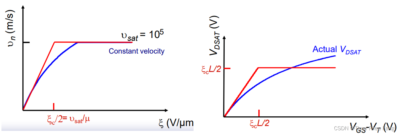
obviously , The above two simplifications are “ Incorrect ” Of , But why is this still the mainstream simplification method ? To illustrate this point , Let's look at a very simple circuit , One is filled to Vdd The capacitance of , In a NMOS Discharge under the control of the tube to 0, because Vgs=Vdd Is constant , and Vds But with the discharge of the capacitor, it continues to decrease , If we plot the flow through the capacitor at this time C Current Id Words , It is not difficult for us to know from the above characteristic curve ,Id It is also a slow decline from saturation , until Vds As small as the transistor returns to the linear region , Approximately linear descent .
however , The delay index we care about in digital circuits , For example, the descent time , It is defined as the time when the voltage drops from the original voltage to half of the original voltage , Corresponding to the characteristic curve of the transistor , The voltage drop of this part is in the speed saturation section , And our simplification errors are mainly in Vds Smaller linear area , When the transistor is in this state , It does not affect the delay characteristics of digital circuits , It can be understood that the switching between high and low levels has been completed , This can be illustrated by the following figure , You can see in the Vds from Vdd drop to Vdd/2 The stage of , Simplify the model and SPICE The error of the model is actually very small . Using the simplified model can greatly save EDA Optimization time of tools .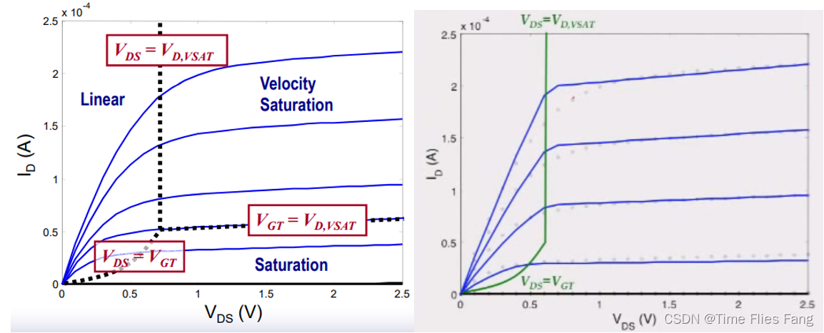
Summary
This section mainly starts from MOS Tube structure , working principle , physical characteristics , Simplify the modeling method by several dimensions , The most basic building units of digital integrated circuits are briefly described , Limited to space , Many details cannot be described , If you want to know more about this part, you can check it by yourself EE141 Courseware and video , You can also learn from classic textbooks 《Digital Integrated Circuit: A Design Perspective》 Further study in .
边栏推荐
- 第六章:云数据库
- Network knowledge corner | it only takes four steps to teach you to use SecureCRT to connect to ENSP. You must see the operation guide of common tools
- 2022-07-26: what is the output of the following go language code? A:5; B:hello; C: Compilation error; D: Running error. package main import ( “fmt“ ) type integer in
- There are two solutions for the feign call header of microservices to be discarded (with source code)
- The data in echart histogram is displayed at the top of the chart
- 第4章 Bean对象的作用域以及生命周期
- 5.component动态组件的展示
- Influxdb basic understanding
- 微信小程序编辑头像
- GenericServlet为什么有两个init方法
猜你喜欢

JS day 2 (variables, variable usage, naming rules, syntax extensions)

干货 | 独立站运营怎么提高在线聊天客户服务?

The price reduction of iphone13 is just a show. Consumers are waiting for iphone14

Okaleido ecological core equity Oka, all in fusion mining mode

数字中国建设峰会闭幕,现场海量图片一览!
深度学习领域图像分割FCN(Fully Convolutional Networks for Semantic Segmentation)

Yolov4网络详解
JS第二天(变量、变量的使用、命名规则、语法扩展)

VSCode开启Pull Request更新代码分支可视化新篇章

IP第十四天笔记

随机推荐
F - Pre-order and In-order(Atcoder 255)
Cloudcompare & PCL matching point median (or standard deviation) distance suppression
Head detached from origin/... Causes push failure
redux三大核心
Title: there is an array that has been sorted in ascending order. Now enter a number and ask to insert it into the array according to the original rule.
Database leader Wang Shan: strive for innovation and carefully Polish high-quality database products
Introduction to regular expressions of shell, general matching, special characters: ^, $,., * Character range (brackets): [], special characters: \, matching mobile phone number
els 兼容性DC、传递图片到窗口
题目:有一个已经按升序排好序的数组。现输入一个数,要求按原来的规律将它插入数组中。
Solution to the third game of 2022 Hangzhou Electric Multi school league
在有序数组找具体某个数字
ROS camera calibration sensor_ Msgs/camerainfo message data type and meaning
结构型模式-桥接模式
[hcip] redistribute, redistribute and redistribute experiments
哈希表刷题(下)
What is the difference between using varchar type and using date type for timestamp column?
【独立站建设】跨境电商出海开网店,首选这个网站建设!
Shell中的文本处理工具、cut [选项参数] filename 说明:默认分隔符是制表符、awk [选项参数] ‘/pattern1/{action1}filename 、awk 的内置变量
Why does genericservlet have two init methods
Eureka service registry