当前位置:网站首页>FPGA interview topic notes (I) - FPGA development process, metastable state and competitive risk, build and hold time, asynchronous FIFO depth, etc
FPGA interview topic notes (I) - FPGA development process, metastable state and competitive risk, build and hold time, asynchronous FIFO depth, etc
2022-06-11 06:16:00 【Fighting_ XH】
List of articles
- 1、 master FPGA Development process
- 2、 How to solve the timing problem
- 3、 Set up time Tsu And hold time Th
- 4、 Clock offset and clock jitter
- 5、 Calculation method of minimum working cycle and maximum working frequency
- 6、 Briefly describe the difference between a trigger and a latch
- 7、 Synchronous and asynchronous circuits
- 8、 asynchronous FIFO Depth calculation
- 9、 Moore and Millie state machines
- 10、FPGA Internal structure resources
- 11、 about IC Design front end 、 Back end understanding
This paper aims at Leetcode in 2021 Autumn moves figures IC Summary of examination questions for design post To study , A lot of knowledge is FPGA Basic learning summary series I have learned , Therefore, when you encounter the same problem, you can only briefly describe .
Click on 2021 FPGA The interview question summary is used to check the questions
Bytes to beat -FPGA post
1、 master FPGA Development process
The following figure for FPGA Development process .
1、 Function definition / Device selection
Simply speaking , This part is to determine the circuit functions to be realized , At the same time, the circuit function is verified before the system design 、 System design and FPGA Choice of chips, etc .
Select design scheme and indicators of device type : According to the mission ( The index and complexity of the system ), To the working speed and the resources of the chip itself 、 Cost, etc , Thus, the design scheme and device type can be selected as an index .
Design method : Generally, the top-down design scheme is adopted , Put the whole system (top top floor ) division , Divided into several basic units , Then each basic unit is divided into basic units of the next layer , Continuous division , Make each input signal , All of them can be used EDA Tools and FPGA Resources design the required output logic .
2、 Design input
This part uses EDA The tool designs the functional circuit . There are generally two ways : Schematic diagram 、HDL Language ,IP nucleus It can also be used as a design input method .
Schematic input : The most direct way to describe , Call the required device directly from the component library , Connect with each other to form a schematic diagram . Intuitive design but inefficient design and inconvenient maintenance , Poor portability .
HDL Language input : Using hardware description language (VHDL、Verilog) Design the functional circuit . Simply speaking , All kinds of logic gates 、 Registers and other circuits are described by the corresponding hardware description language . advantage : Language has nothing to do with chip technology , So in any FPGA On chip , Can be designed with hardware description language , Strong portability .
3、 Functional simulation ( Pre simulation )
Functional simulation is also called pre synthesis simulation , This part is to verify the logic function of the circuit , There is no need to consider delays, etc . Method : To write testbench The test file , After using EDA Tools (modelsim) Conduct waveform simulation And generate a report file , Verify the circuit function according to the waveform .
4、 Comprehensive optimization
Synthesis is aimed at the given circuit function and the constraints of realizing the circuit ( Speed 、 Power waste 、 Cost and circuit type, etc ), Optimize the designed circuit . The result of the synthesis is the design scheme of the hardware circuit , The scheme should meet the expected design requirements of the given circuit .
5、 Post synthesis simulation ( Post simulation )
stay quartus After the hardware description is completed in , Generate function net table after synthesis , Write at this time tb file , Load the written functional circuit into modelsim In the simulation , This is called post simulation , It takes the gate delay parameters of the circuit and the connection conditions between various circuit units into account before simulation , It is mainly used to check whether the comprehensive result is consistent with the original circuit design .
6、 Layout and wiring
After successful post simulation , We need to be in quartus Complete mapping and layout routing in , That is, mapping logic to FPGA On the resources of device structure , in short , Configure the net list generated after synthesis to a specific FPGA On chip , At the same time, ensure the speed 、 The connection mode with optimal area . After this part is completed, we can get the configuration file , And automatically generate reports , obtain FPGA Use of resources .
Static time series analysis : Analyze setup time and hold time .
7、 Time series simulation
Also known as post simulation , Take into account the delay of layout and routing , So as to check whether there is any violation in the timing ( It mainly analyzes whether the time sequence requirements are met , For example, whether the establishment time and holding time are met ).【 Timing simulation includes layout and routing delay , And the time delay is also loaded in the waveform , But the internal delay of different chips is different , Therefore, different layout and routing schemes will also bring different delay effects , So after the layout and wiring , We can simulate the timing of the whole system or each module , To get the temporal relationship , Estimate the performance of the system , It can also check and eliminate competitive risks 】
8、 Board level simulation and verification
Board level simulation is mainly used in high-speed circuit design , Signal integrity of high-speed system 、 Electromagnetic interference and other characteristics are analyzed .
9、 Chip burning and debugging
So far, we have completed the logic circuit design , And the configuration file is generated , Download profile to FPGA Development board , Implement verification and debugging of functions on the development board .
Sum up , Give adoption ZYNQ To realize the whole FPGA Development process Steps for .
2、 How to solve the timing problem
1、 Use static or dynamic timing analysis , To calculate the propagation delay of each path , Check whether the signal establishment time and holding time meet the timing requirements . Through the analysis of maximum path delay and minimum path delay , Identify errors that violate timing constraints . You can also optimize the timing according to the timing report .
2、 To master what timing problems there are , Such as metastable state , Solve the problem .
2.1 Metastable phenomena in sequential logic circuits
You need to know what metastable states are , And how metastable phenomena are produced , How can we solve the problem of metastable state .
Metastable : The input signal changes between the set-up time and the hold time of the effective edge of the clock , It does not meet the timing requirements of trigger establishment and holding time , The output is in an uncertain state for a period of time , This is metastable .
Metastable phenomena include the following :
1、 Metastable state in the cross clock domain : The phase shift between the source signal clock and the destination signal clock is unknown , It may cause that the holding time and establishment time conditions are not met , Thus, metastable state is produced .—— use FIFO Buffer design for cross clock domain data communication .
2、 Metastable state in asynchronous signal : Because the asynchronous signal is not synchronized with the trigger synchronous clock , Therefore, the holding time and establishment time conditions may not be satisfied , Produce metastable state phenomenon .—— Solve the problem by synchronous processing .
3、 Metastable state in asynchronous reset detection : The change of the reset signal occurs within the establishment or holding time , There is no guarantee that Tsu and Th The requirements of , Metastable state appears .—— Asynchronous reset is used for reset circuit 、 Synchronous release mode processing .
Be careful : For single bit data transmission , We can use two registers to synchronize , To consume metastable , But multi bit data needs to be asynchronous FIFO To deal with it , Because the synchronizer output can only ensure that the final output is a steady state ,0 perhaps 1, But there is no guarantee that it is a definite value . Therefore, if the multi bit data is synchronized to eliminate the metastable state , There will be garbled code .
It is enough to check the metastable state .
Time series convergence method
Clock crossing problem
2.2 The delay of combinational logic is too large to meet the requirements
Insert registers to shorten the delay of combinational logic .( Assembly line technology 、 Parallel design )
2.3 Competition and adventure in combinatorial logic
2.3.1 What is competition and adventure
competition (Competition): In combinational logic circuits , An input variable passes through multiple lines ( Two or more ) Path to output , Because the delay time of each route is different , The time to reach the output gate is first and then , This phenomenon is called competition . Competition is divided into critical and non critical competition , The competition that will not produce error output is non critical competition . The competition that produces temporary or permanent errors is the critical competition .
adventure (risk): When the signal passes through the wiring and logic unit inside the device , There is a certain delay . The delay time is related to the length of the connection and the number of logical units , It is also affected by the manufacturing process of the device 、 voltage 、 Temperature, etc ;
Multiple signals also have different delays when the level value changes , Corresponding The output of combinatorial logic has a sequence , So there is risk .
There will be some incorrect spikes in the phenomenon of adventure , be called " skin needling ". If a combinational logic circuit has " skin needling " appear , It shows that there is a risk in the circuit . It can also be said that the circuit output has instant error due to competition , This phenomenon is risky .
2.3.2 The reasons causing
summary : Competition and risk are caused by circuit delay , At the same time, risk is caused by competition , And the competition is because the delay in the circuit is different , But when there's competition, there's no risk .
subject :( Dajiang 2020 Chip Engineer Recruitment ) The adventure in combinational logic is due to ( D) Caused by the .
A、 The circuit has multiple outputs
B.、 The circuit is not minimalist
C、 Logic gate types are different
D、 Time delay in a circuit
An example is given below to explain :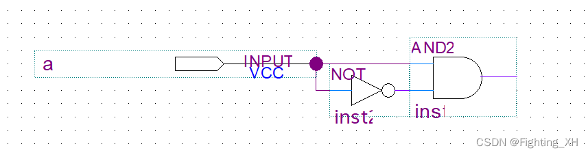
As can be seen from the picture above , Implemented function out = a & (~a); The design appears 1 adventure , That is, the result itself should be 0, But there is a phenomenon called 1 Burr of , Therefore 1 adventure .
2.3.3 Judgment method
Algebra :
In logical function expression , If a variable is represented by Primitive and inverse variables There are two forms .
If the expression is :Y=A+A’, It will produce “0” adventure ;F=A*A’, It will produce “1” adventure .( The result should be 1 appear 0 The error is 0 adventure , Instead of 1 adventure )
Karnaugh map method :
If the input variable changes in the neighborhood of the adjacent Karnaugh circle , And it's going from one Karnaugh circle to another , It may lead to logical adventure .( The Karnaugh map is tangent )
As can be seen from the picture above , There are two tangent but disjoint cycles in a Karnaugh map , Then there will be risk-taking when exporting .
2.3.4 resolvent
(1) Add redundancy
According to kanotu, we can see , We added a circle , Logical expressions are not the simplest , But it can eliminate risk situations .
(2) Add strobe signal ( High level )
A strobe signal is added to the input , in the light of A+(~A) Of 1 Risk taking , Avoid burrs .
(3) Introducing a blocking pulse ( Low level )
The input is added with blocking pulse signal , in the light of A·(~A) Of 0 Risk taking , Avoid burrs .
(4) Increase the filter capacitance
Because the risk output is a very narrow burr , Therefore, a filter capacitor can be connected at the output end to filter it .
(5) Using reliability coding
For example, the coding method of gray code , Every time it changes, it only changes 1 position .
3、 Set up time Tsu And hold time Th
In the static timing analysis part, the setup time and hold time are explained .
Setup time and hold time are discussed in sequential logic circuits , Both are used to test whether the time requirements between the input signal and the clock signal are met .
Establish and maintain time according to the following figure :
Tsu Set up time for : Before the rising edge of the trigger comes , The minimum time for the input data to remain unchanged is Tsu. if Tsu Not meeting the requirements , So the input signal data The trigger cannot be entered correctly on this clock , Need to wait for the next rising edge of the clock .
Th To keep time : After the rising edge of the clock appears , The minimum time for data to remain stable is the holding time , If holding time is not enough , Then the data can not be correctly entered into the trigger .
therefore D The data input by the trigger must reach... Before the establishment time , And last until after the holding time .

3.1 It works / Inherent build time and hold time
Suppose the effective holding time is Tsetup_valid.
about D trigger , Its own establishment time Tsu = 2ns, That is, the data is kept until the effective edge of the clock comes 2ns The stability of the , In this way, it can be ensured that the input from datatin The data arrived steadily D End .
Because the clock comes from clock, There is also a clock delay , And clk Before the trigger Toffest=1ns arrive .
therefore , Consider clock delay , Get effective hold time :Tsetup_valid = Tsu - Toffest = 1ns
.
Consider data path latency , obtain Tsetup_valid = Tsu - Toffest +Tcmob
Effective holding time Thold_valid The same analysis .
Consider the effect of clock delay :
Consider that the circuit clock arrives earlier than the trigger clock Toffest = 1ns, So the effective holding time of the circuit Thold_valid = Thold + Toffest ;
.
Consider the impact of path delay :Data needs to go through a period of combinatorial logic before it can remain stable , Therefore, the effective holding time of the circuit is :
Thold_valid = Thold + Toffest - Tcmob
3.2 The essence of timing design
Meet the requirements of each trigger establishment time and holding time
3.3 Formulas for establishing and maintaining time margin
Establish time margin formula :
T slack = Tclk + Tskew - Tsu - Tco - Tcomb;
Hold time margin formula :
T slack = Tco + Tcomb - Tskw - Th
4、 Clock offset and clock jitter
4.1 Concept
Master clock offset (Tskew) And clock jitter (Tjitter) What are the differences , And how to reduce the occurrence of these two situations .
Clock offset is the difference between two different flip flops when the same clock arrives .Tskew = Tclk2 - Tclk1
Clock jitter is the difference between two clock cycles .Tjitter=T2 - T1
4.2 If you reduce clock offset and clock jitter
Methods to reduce clock jitter :
Affected by the clock itself , Not affected by wiring , Therefore, by controlling the temperature change of the system 、 Reduce mechanical vibration 、 Reduce power 、 And so on to reduce , Choose a good clock source .
Methods to reduce clock offset :
Clock offset is due to wiring length or different loads ( Combinatorial logic ) Caused by the , Therefore, a clock driver with low output impedance can be used , If the driving capacity is not enough, the power supply of the same model can be connected in parallel 、 Adopt tree structure 、 Low impedance clock distribution line 、 Remote matching multiple drivers to solve .—— Adopt global clock
Add :
In a general way , When we divide the frequency , use PLL To complete , Try to avoid logical operation of the clock , Otherwise, clock offset may occur 、 shake , Even clock glitches occur .
5、 Calculation method of minimum working cycle and maximum working frequency
 Minimum duty cycle Tmin=Tco+Tcomb+Tsu-Tskew+ Tjitter // Register internal delay + Combinatorial logic delays + Establish time delay - Clock offset  +  Clock jitter
 Maximum operating frequency 1/Tmin
 Be careful : In solving Tcmob When  , Find the critical path between the two triggers
In order to better understand , Give the following example :
As shown in the figure , Both registers and logic blocks are unit delay ,Tr = Tf = 1; A register is a rising edge trigger , The establishment time is Tsu = 1, Multiplexer MUX The delay of is Tmux = 2.
(1) Regardless of clock deviation , Calculate the minimum clock cycle
First, we choose the longest path to calculate the minimum clock cycle :
Tmin = Tco+Tcomb+Tsu = 1+ 1*5 + 2 + 1 = 9;
(2) Consider clock offset and Tskew = t2 - t1 = 1 When , Minimum clock period :
Tmin = Tco+Tcomb+Tsu-Tskew = 1+ 1*5 + 2 + 1 -1 = 8;
(3) Consider clock offset and Tskew = t2 - t1 = 4 When , Minimum clock period :
Tmin = Tco+Tcomb+Tsu-Tskew = 1+ 1*5 + 2 + 1 -4 = 5; But because of (1) We can see , Regardless of clock skew , The minimum clock cycle is 7, If less than 7, Then the register cannot sample correctly , So the question is (3) Under the circumstances , The minimum clock cycle is 7
(4) Suppose the clock cycle T, The allowable clock deviation range that can ensure the normal operation of the circuit is derived ( Consider the positive and negative clock deviation )
Tskew = t2 -t1 ;
 When the deviation is positive : If you want to R2 Sample the data correctly , Then the clock deviation must be less than R1 To R2 Minimum delay of , be  Tskew < 1+1*3+2 = 6 ( The establishment time is not included )
 Negative deviation :T - |Tskew| ≥ R1 To R2 The maximum delay of   therefore ,T - |Tskew|  ≥ 9
 So I got :
(9-T) ≤ T_skew < 6
6、 Briefly describe the difference between a trigger and a latch
trigger : Clock edge trigger ( Sequential logic circuit ), Trigger a state change at the edge of the clock .
Latch : Level trigger ( Combinational logic circuit ), Trigger state change under the action of input level .
Tell the difference in detail
7、 Synchronous and asynchronous circuits
7.1 Synchronous logic and asynchronous logic ( Han Wang )
Synchronous logic : There is a fixed causal relationship between clocks
There is a fixed causal relationship between the synchronous logic circuit and the clock , The clock terminals of all flip flops in the circuit are connected together , And connected to the clock end of the system , Only when the clock pulse comes , The state of the circuit can be changed , Otherwise keep , Independent of changes in input .
Add : Adopted PLL The frequency division circuit can also belong to the synchronous logic , Because although the frequency division gets different clocks , But their system clocks are the same .
Asynchronous logic : There is no fixed causal relationship between clocks
There is no uniform clock in the circuit , The state of the circuit changes depending on the external input changes .
7.2 The difference between synchronous reset and asynchronous reset
1、 Synchronous reset :
Reset signal and clk It works , When clk When it works , Reset is effective .
advantage : It is conducive to time series analysis ; Because only in clk It works when it works , Therefore, the burr phenomenon can be prevented .
shortcoming : The reset signal must be greater than the clock cycle , Can be truly recognized by the system ; In most logic devices D All triggers have only asynchronous reset ports , Therefore, if synchronous reset is adopted , You need to insert combinational logic into the data input of the register , At this point, we need to consider the delay of combinatorial logic and other factors .
module test(clk,rst,q,d);


	 input           clk    ;
	 input           rst    ;
	 input           d      ;
	 output  reg     q      ;


always @ (posedge clk  )
    if(rst)
	     q <= 0;

    else
	     q <= d;

endmodule

2、 Asynchronous reset :
Reset signal and clk irrelevant , It is only related to the reset signal input by itself .
advantage : In most logic devices D All triggers have only asynchronous reset ports , There is no need to insert combinatorial logic , Provincial resources ; The design is relatively simple ;
shortcoming : The reset signal may not meet the set-up and hold time requirements , Therefore, metastable states are prone to occur ; Susceptible to burrs ;
module test(clk,rst,q,d);


	 input           clk    ;
	 input           rst    ;
	 input           d      ;
	 output  reg     q      ;


always @ (posedge clk or posedge rst )
    if(rst)
	     q <= 0;

    else
	     q <= d;

endmodule

Add : If the circuit uses the same clock source , But in the sub module, the PLL The divided clock is used to drive , This is still a synchronous circuit , Therefore, the whole circuit is driven by a unified clock source . There is no uniform clock source for asynchronous circuits .
With synchronization 、 Asynchronous trigger reference .
8、 asynchronous FIFO Depth calculation
FIFO Used to buffer block data streams , Usually when writing is fast and reading is slow .
8.1 Time of data transmission = FIFO Fill in the time
The formula :
FIFO Full time = Time of data transmission
FIFO Fill in the time = FIFO depth / ( Write rate - Readout rate )
Data transfer time = Data volume / Write rate
therefore :
FIFO depth / ( Write rate - Readout rate )= Data volume / Write rate
Give an example :
Now we need to pass A Write 10 All the data , And send it to by reading the clock B, Write clock 50Mhz, Read the clock as 40mhz, If you want data not to be lost , So you need to AB Insert between FIFO, So how deep do we need to insert FIFO Well ?
Time of data transmission = Data volume / Write rate
therefore
Time of data transmission = 100000 / 50mhz = 1 / 500s = 2ms
Time of data transmission = FIFO Fill in the time = FIFO depth / ( Write rate - Readout rate )
therefore 2ms = depth / 10mhz
FIFO depth = 20k
8.2 depth = The amount of data written - Read data volume
subject :
It is known that : clock frequency :clkA = clkB / 4 ; Clock cycle :clk (en_B) = clkA * 100 ;en_B Duty ratio 25%. seek FIFO depth .
Explain :
hypothesis clkA = 100 MHz ,clkB = 400Mhz, be TclkA = 10ns,TclkB = 2.5ns, Empathy en_B Period is clkA Of 100 Multiple , therefore Ten = 1000ns
because enB Duty ratio 25%, Therefore, the high level of the signal continues 250ns.
hypothesis clkA To read the clock ,clkB Write clock for , When enB When it's high level , Use the write clock to start writing data , Amount of data written = 250ns / 2.5ns = 100 Data .
When write enable is effective , With data , Therefore, read operation can be performed , Reading data = 250ns / 10ns = 25 Data
depth = Write data - Read the data = 75
therefore FIFO Depth is 75.
9、 Moore and Millie state machines
Both are sequential logic circuits .
1、Moore The output of the state machine is only related to the current state value , And only when the edge of the clock comes will there be a state change .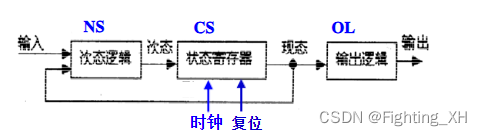
2、Mealy The output of the state machine is not only related to the current state value , And related to the current input value .
3、 What is a state diagram ?
The state diagram describes the state transition law of sequential logic circuit and the relationship between output and input in the form of geometry .
Master the difference between the two state machines
Master a paragraph 、 How to write two-stage and three-stage state machines
10、FPGA Internal structure resources

11、 about IC Design front end 、 Back end understanding
Design front end is also called logic design , Back end design is also called physical design .
Front end design : Requirements analysis and architecture design 、 take HDL Language –> Net watch ,RTL Design 、 Simulation verification 、 Logic synthesis
Back end design : Net watch –> Chip layout . Layout, wiring and board level physical verification .
Continue to learn FPGA Interview topic notes ( Two ) Well
边栏推荐
- Use of constructors
- Managing VHDS using batch
- Super details to teach you how to use Jenkins to realize automatic jar package deployment
- What do you need to know about Amazon evaluation?
- Sign for this "plug-in" before returning home for the new year
- Experimental report on information management and information system [information security and confidentiality] of Huazhong Agricultural University
- Basic use of BufferedReader and bufferedwriter
- 通过R语言且只用基础package来制作一个小游戏
- Principle of copyonwritearraylist copy on write
- jenkins-用户权限管理
猜你喜欢

Which company is better in JIRA organizational structure management?

Yonghong Bi product experience (I) data source module
Devsecops in Agile Environment

ERROR 1215 (HY000): Cannot add foreign key constraint

“All in ONE”一个平台解决所有需求,运维监控3.0时代已来

Notes sur les questions d'entrevue de la FPGA (IV) - - détecteur de séquence, Code gris dans le domaine de l'horloge croisée, opération de ping - pong, réduction de la perte statique et dynamique, err

Sword finger offer 50: the first character that appears only once

Servlet
Servlet

Shandong University machine learning experiment VI k-means
随机推荐
Twitter data collection (content, fans, keywords, etc.)
Squid agent
Devsecops in Agile Environment
Use of constructors
All the benefits of ci/cd, but greener
autojs,读取一行删除一行,停止自己外的脚本
Delegation agreement, data source agreement and advanced view in view
Using Internet of things technology to accelerate digital transformation
Teach you to write word formula
MySQL implements over partition by (sorting the data in the group after grouping)
ThymeleafEngine模板引擎
Login and registration based on servlet, JSP and MySQL
Notes sur les questions d'entrevue de la FPGA (IV) - - détecteur de séquence, Code gris dans le domaine de l'horloge croisée, opération de ping - pong, réduction de la perte statique et dynamique, err
我们真的需要会议耳机吗?
On the social moral and ethical issues behind short videos (personal point of view, for reference only)
Excellent practice | how to avoid a bloody case caused by a line of wrong code?
[usual practice] explore the insertion position
Simple knapsack problem
The classification effect of converting video classification data set to picture classification data set on vgg16
Can Amazon, express, lazada and shrimp skin platforms use the 911+vm environment to carry out production number, maintenance number, supplement order and other operations?