当前位置:网站首页>FPGA based analog I ² C protocol system design (Part I)
FPGA based analog I ² C protocol system design (Part I)
2022-06-24 15:11:00 【FPGA technology Jianghu】
be based on FPGA The simulation I²C Protocol system design ( On )
Today, I bring you FPGA Of simulation I²C Protocol design , Because of the long space , It is divided into three parts . Today I bring the first one , Part 1 , I²C Bus analysis and simulation I²C Basic framework of interface program . Don't talk much , Loading .
There are also related articles before , Great Xia, you can search by yourself , Source series : be based on FPGA Of IIC Design ( Source attached works ).
Reading guide
I²C(Inter-Integrated Circuit), It's actually I²C Bus abbreviation , Chinese is integrated circuit bus , It's a serial communication bus , Using multi master slave architecture , By Philips in 1980 In order to make motherboard 、 Embedded systems or mobile phones are developed to connect low-speed peripheral devices .I²C The correct reading of is “I square C”("I-squared-C"), and “I Two C”("I-two-C") Is another wrong but widely used way of reading . since 2006 year 10 month 1 The date of , Use I²C The agreement no longer requires the payment of patent fees , But manufacturers still have to pay for I²C Slave device address .
I²C Simply speaking , Is a serial communication protocol ,I²C The communication protocol and communication interface are widely used in many projects , Such as serial in the field of data acquisition AD, Camera configuration in the field of image processing , In the field of industrial control X X-ray tube configuration, etc . besides , because I²C The agreement occupies IO There are very few resources , Easy to connect , Therefore, it is often used in engineering I²C The interface is used as the communication protocol between different chips .I²C A serial bus usually has two signal wires , One is a two-way data line SDA, The other is the clock line SCL. All received I²C Serial data on the bus device SDA All connected to the bus SDA On , Clock line of each device SCL Connected to the bus SCL On .
In modern electronic systems , There are numerous IC Need to communicate with each other and with the outside world . In order to simplify the circuit design ,Philips The company has developed an internal IC Simple bidirectional two-wire serial bus for control I²C(Intel-Integrated Circuit bus).1998 When launched in I²C bus protocol 2.0 version ,I²C The agreement has actually become an international standard .
It's going on FPGA When the design , It is often necessary to provide with the periphery I²C Interface chip communication . For example, low power consumption CMOS Real time clock / Calendar chip PCF8563、LCD Driver chip PCF8562、 Parallel port expansion chip PCF8574、 keyboard /LED Driver ZLG7290 And so on I²C Interface . So in FPGA Middle simulation I²C The interface has become FPGA Develop the necessary steps .
This article will explain in detail in FPGA The chip uses VHDL/Verilog HDL simulation I²C agreement , And compiling TestBench Methods of simulating and testing programs .
The first content abstract : Introduction I²C Bus analysis , Include I²C Bus Overview 、I²C The basic concept of agreement 、I²C Timing requirements of the protocol , Simulations are also introduced I²C Basic framework of interface program and other related contents .
One 、I²C Bus Overview
Let's start with I²C The data format and timing in the protocol are introduced , For places not covered here, please refer to 《THE I²C-BUS SPECIFICATION VERSION 2.1 JANUARY 2000》.
1.1 I²C Bus Overview
I²C As a serial bus standard, the protocol has no data throughput capability of parallel bus , But its following characteristics make it widely used :
- Just two buses — Serial data line SDA And serial clock line SCL;
- Each device connected to the bus can pass through a unique address and a simple host that always exists / Set the address from the node relationship software , The master node can send or receive data ;
- It is a true multi master bus , When two or more master nodes initiate data transmission at the same time , Data corruption can be prevented through conflict detection and arbitration ;
- Serial 8 Bit rate can be achieved in standard mode 100kbit/s, It can be reached in fast mode 400kbit/s, It can be reached in high speed mode 3.4Mbit/s;
- The on-chip filter can filter out the hairy spikes on the bus data line , Ensure data integrity ;
- Connected to the same bus IC The quantity is only affected by the maximum capacitance of the bus (400pF) Limit .
A bus is more than just an interconnect , It also contains all the formats and processes of system communication .I²C The characteristics of bus structure ensure the simplicity of its application , In addition, its complete protocol avoids all confusion 、 The possibility of data loss and obstruction of information .
1.2 I²C The basic concept of agreement
I²C The bus supports any IC Production process (NMOS、CMOS And bipolar ). Serial data line SDA And serial clock line SCL Transfer information between devices connected to the bus . Each device has a unique address as an identification mark ( Whether it's a microcontroller 、LCD Drive memory or keyboard interface ), And both can send and receive data . Obviously LCD The drive only needs to receive data , The memory needs to receive and send data . chart 1 Shown is an example of a high-performance integrated TV .
chart 1 High performance integrated TV
From the picture 1 You can see , application I²C The bus is very convenient . In popular words I²C The hardware design of the bus is to connect SDA and SCL Two lines , rely on I²C The agreement completes the software work . stay I²C The following concepts shall be understood in the agreement .
1) Lord / From the node
The master node is responsible for initializing the data transmission of the bus , And generate a clock signal that allows transmission . At this time, any addressed device is considered as a slave node . When there are multiple master nodes transmitting data on the bus , Each master node generates its own clock signal . All peripheral devices attached to the bus 、 Peripheral interfaces are nodes on the bus .
2) Addressing mode of nodes on the bus
There is only one master on the bus at any time ( Master node ) Realize the control operation of the bus , Addressing other nodes on the bus , Timesharing implementation point - Point data transmission . Therefore, each node on the bus has a fixed node address .
I²C The address of the master node on the bus is given by the software , This address is stored in I²C In the address register of the bus .I²C All peripheral devices on the bus have standard device addresses . The device address consists of 7 Digit composition , It and 1 Bit direction bits constitute I²C Addressing bytes of bus devices SLA(Slave address).
The device address is I²C Address coding inherent in bus peripheral interface devices , The device is given at the factory . The data direction bit specifies the data transmission direction of the master node to the slave node on the bus .
1.3 I²C Timing requirements of the protocol
1) Data transfer timing on the bus
I²C The data transmission sequence on the bus is shown in the figure 2 Shown , The specific steps are as follows .
chart 2 I²C Bus data transfer timing
- First, the master node device sends a start signal .
- Next, the master node device sends the slave node address and the read / write mode , altogether 8 position . Where the slave node address 7 position , How to read and write 1 position .
- The slave device corresponding to the transmission address responds ( namely ACK).
- Start data transfer , There is no limit to the amount of data transmitted . Every byte ( Octet ) Followed by the reply bit of the receiving data party . For example, the master node device reads the slave node data , Send data from node , Master node response ; The master node device writes data to the slave node , The master node sends data , Answer from node .
- End of data transfer , The master node device sends a termination signal to end the whole process .
use I²C There is no limit on the number of bytes transferred after the bus , It only requires the other party to respond to a reply bit after each byte is transmitted . The highest bit of data is sent first (MSB,Most Significant Bit). There is a start signal at the beginning of each transmission , There is a stop signal at the end . After the bus transfers a byte , Through the clock line (SCL) The control of causes the transmission to be suspended . For example, when a peripheral device receives N A period of processing time is required after a byte of data in order to continue to receive subsequent byte data , At this time, after answering the signal, you can make SCL Change to low level control bus pause . If the master node requires bus pause, the clock line can also be kept low to control bus pause .
2) Timing signals on the bus
I²C The bus is a synchronous transmission bus , The bus signal is fully synchronized with the clock .I²C The signals related to data transmission on the bus have start signals S、 Stop signal P、 Answer signal A And bit transfer signal . These signals will be introduced one by one .
(1) Start signal
Start signal (Start Condition) Pictured 3 Shown . At that time, the clock line SCL For high voltage , cable SDA The change from high level to low level will form the starting signal , start-up I²C Bus .
(2) Stop signal
Stop signal (Stop Condition) Pictured 3 Shown . At that time, the clock line SCL For high voltage , cable SDA Changing from low level to high level will form a termination signal , stop it I²C Bus .
(3) Answer signal
Pictured 3 By ACK The first 9 Clock pulses correspond to reply bits , The low level on the corresponding data line is the response signal , High level is a non response signal .
chart 3 Start signal and end signal
(4) Bit transmit signal
stay I²C After the bus is started or after the reply signal 1~8 One clock pulse corresponds to one byte 8 Bit data transfer . During pulse high level , Data serial transmission ; Prepare for data during low level , Allow data level conversion on the bus .
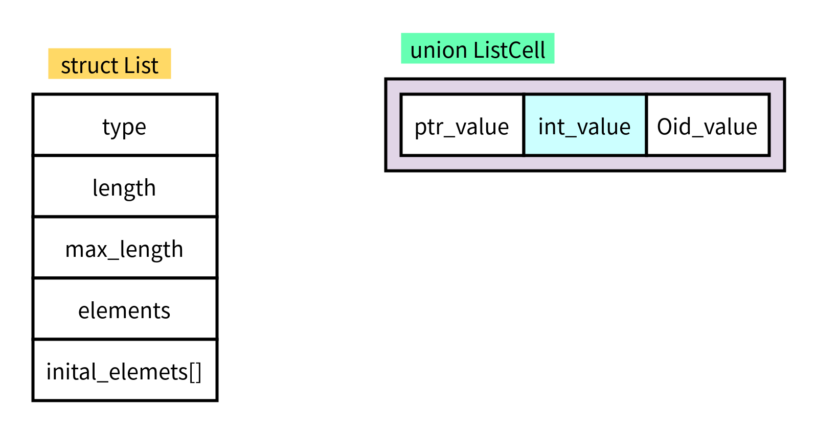
Two 、 simulation I²C Basic framework of interface program
simulation I²C The basic framework of the interface program is shown in Figure 4 Shown .
chart 4 simulation I²C Basic framework of interface program
1) Program interface
Interface for connecting with the application , The data of the application is divided into I²C By agreement SDA To external devices . Include the following :
- clk_I FPGA External clock signal .
- rst_I Synchronous restart signal .
- arst_I Asynchronous restart signal .
- adr_I Slave node address .
- dat_I input data .
- dat_o Output data .
- we_I Write valid signal .
- stb_I Interface valid signal .
- cyc_I Valid bus cycle input .
- ack_o Reply signal output .
- inta_o Interrupt signal output .
2) Clock setting register
I²C The agreement provides 3 Two speed modes : Normal speed mode 100kbit/s、 Fast mode 400kbit/s、 High speed mode 3.5Mbit/s.SCL The frequency of the output clock signal is consistent with the speed mode . Program internal use 5 times SCL The signal acts as a clock , and FPGA The external clock needs to be divided to get the clock used internally by the program .
for example : Use normal speed 100kbit/s,FPGA The external clock is 50MHz, Then the clock setting register needs to be set to (50MHz/5*100kHz – 1=99).
3) Clock generation module
The clock generation module generates 4 times SCL Frequency clock signal , It provides trigger signals for all synchronous actions in the bit transmission control module .
4) Command register
The command register consists of 8 position , It determines whether various timing signals are generated on the bus 、 Read or not / Writing data , The meanings expressed by you are shown in the table 1 Shown .
surface 1 Command register contents
5) Status register
The status register is used to display the status of the current bus , For example, whether a response signal from the slave node is received 、 Are you busy 、 Whether it is transferring data, etc , The specific contents are shown in the table 2 Shown .
surface 2 Status register contents
6) Data transfer register
The data transfer register is used to store the data waiting to be transferred . When passing slave node address information , front 7 Bit saves the slave node address , The last bit saves the read / write command ; When passing ordinary data ,8 Bit holds a byte of data . The specific contents of the data transmission register are shown in table 3 Shown .
surface 3 Data transfer register contents
7) Data receiving register
The data receiving register is used to save the pass I²C The last byte received by the bus , The specific contents are shown in the table 4 Shown .
surface 4 Contents of data receiving register
8) Byte transfer control module
The byte transmission control module controls in bytes I²C Bus data transmission . This module passes the contents of the data transfer register to according to the contents set in the command register I²C The receiving end of the bus , Or from I²C The bus sending end receives the data and saves it in the data receiving register .
9) Bit transfer control module
The bit transmission control module performs in bits I²C Bus data transmission and generation I²C Agreement order ( As in the beginning 、 stop it 、 Repeat start, etc ). The byte transmission control module controls various actions of the bit transmission control module . For example, read a byte of data , The bit transfer control module needs to perform 8 A read command .
10) Data shift register
The data stored in the data shift register is always related to the current data transmission . For example, when reading , The master node passes through the shift register in turn SDA Get it from I²C Data from the sender , After completion, the data is copied to the data receiving register . When writing , The data in the data transfer register is copied to the data shift register , And then one by one SDA Transfer data to I²C The receiving end of the bus .
This is the end of this article , The next one is based on FPGA The simulation I²C Protocol design ( in ),I²C The concrete realization of the agreement , Including the implementation of bit transmission 、 The realization of byte transmission and the realization of program body .
边栏推荐
- The security market has entered a trillion era, and the security B2B online mall system has been accurately connected to deepen the enterprise development path
- 动作捕捉系统用于地下隧道移动机器人定位与建图
- 安装wireshark时npcap怎么都安装不成功,建议先用winpcap
- Huangchuping presided over the video conference on fixed-point contact with Zhuhai, resolutely implemented the deployment requirements of the provincial Party committee, and ensured positive results i
- Online text entity extraction capability helps applications analyze massive text data
- update+catroot+c000021a+critical service failed+drivers+intelide+viaide+000000f
- [environment setup] zip volume compression
- Stm32f1 and stm32cubeide programming examples -ws2812b full color LED driver (based on spi+dma)
- 09_ An efficient memory method
- Linux 安装 CenOS7 MySQL - 8.0.26
猜你喜欢

laravel下视图间共享数据
Data sharing between laravel lower views

Virtual machines on the same distributed port group but different hosts cannot communicate with each other

MySQL log management, backup and recovery
postgresql之List
Wide measuring range of jishili electrometer

从pair到unordered_map,理论+leetcode题目实战

Bert whitening vector dimension reduction and its application

`Thymeleaf ` template engine comprehensive analysis
GO语言-goroutine协程的使用
随机推荐
一个简单而功能强大的开发者工具箱Box3.cc
【比特熊故事汇】6月MVP英雄故事|技术实践碰撞境界思维
Carry forward the fine style of continuous operation and go all out to ensure the safety of Beijiang Levee
ES mapping之keyword;term查询添加keyword查询;更改mapping keyword类型
Cvpr2022 𞓜 thin domain adaptation
MySQL title
六月集训(第23天) —— 字典树
入行 4 年,跳槽 2 次,我摸透了软件测试这一行
[environment setup] zip volume compression
tongweb使用之端口冲突处理办法
In the eyes of the universe, how to correctly care about counting East and West?
Mots clés pour la cartographie es; Ajouter une requête par mot - clé à la requête term; Changer le type de mot - clé de cartographie
Virtual machines on the same distributed port group but different hosts cannot communicate with each other
[ansible problem processing] remote execution user environment variable loading problem
Data sharing between laravel lower views
Is it safe to open an account in flush? What preparation is needed
An accident caused by a MySQL misoperation, and the "high availability" cannot withstand it!
Keras deep learning practice (11) -- visual neural network middle layer output
GO语言并发模型-MPG模型
Is financial management of securities account safe??