当前位置:网站首页>FPGA_ Initial use process of vivado software_ Ultra detailed
FPGA_ Initial use process of vivado software_ Ultra detailed
2022-07-26 02:52:00 【SmallCloud#】
It should be noted that : I'm using the version 2018.2, Different versions of software may differ
Introduction to the development process : Open software — New project — Design input — Analysis and synthesis — Constraint input — Design implementation — Generate and download bitstreams
1、 Open software , Click on Quick Start Under the Create Project

2、 Pop up and click NEXT

3、 Fill in the project path and project name and click NEXT( Note that the path should not contain Chinese )

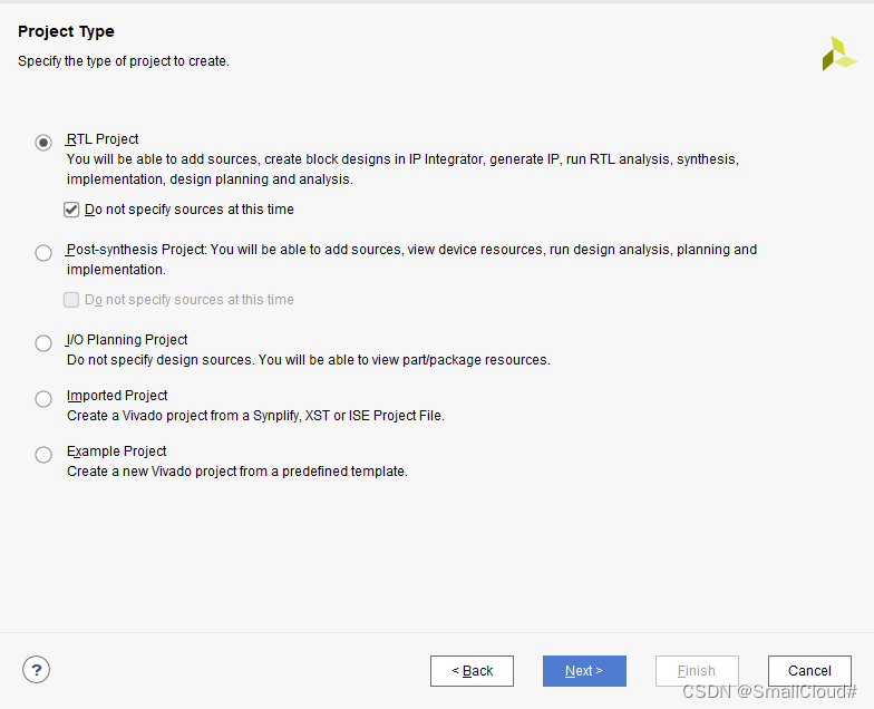
4、 choice RTL project, Check do not specify sources at this time Indicates that the source file is not specified , Click on next
5、 choice FPGA Click next
You can filter through the options above , You can also enter the model directly to search

6、 single click Finish

7、 Click on + Add new file

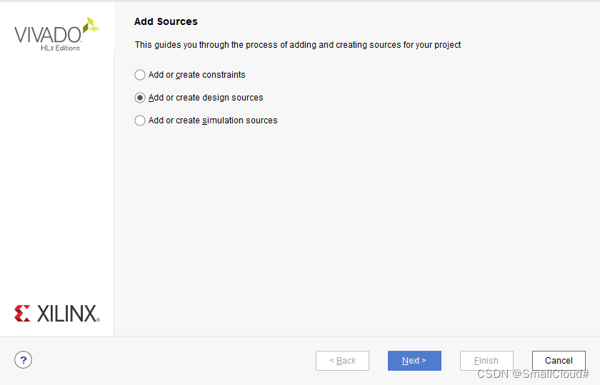
8、 choice add or create design sources Back click NEXT
9、 single click Create File, Input file name XXX Then click OK

10、 single click Finish —> single click OK —> single click Yes

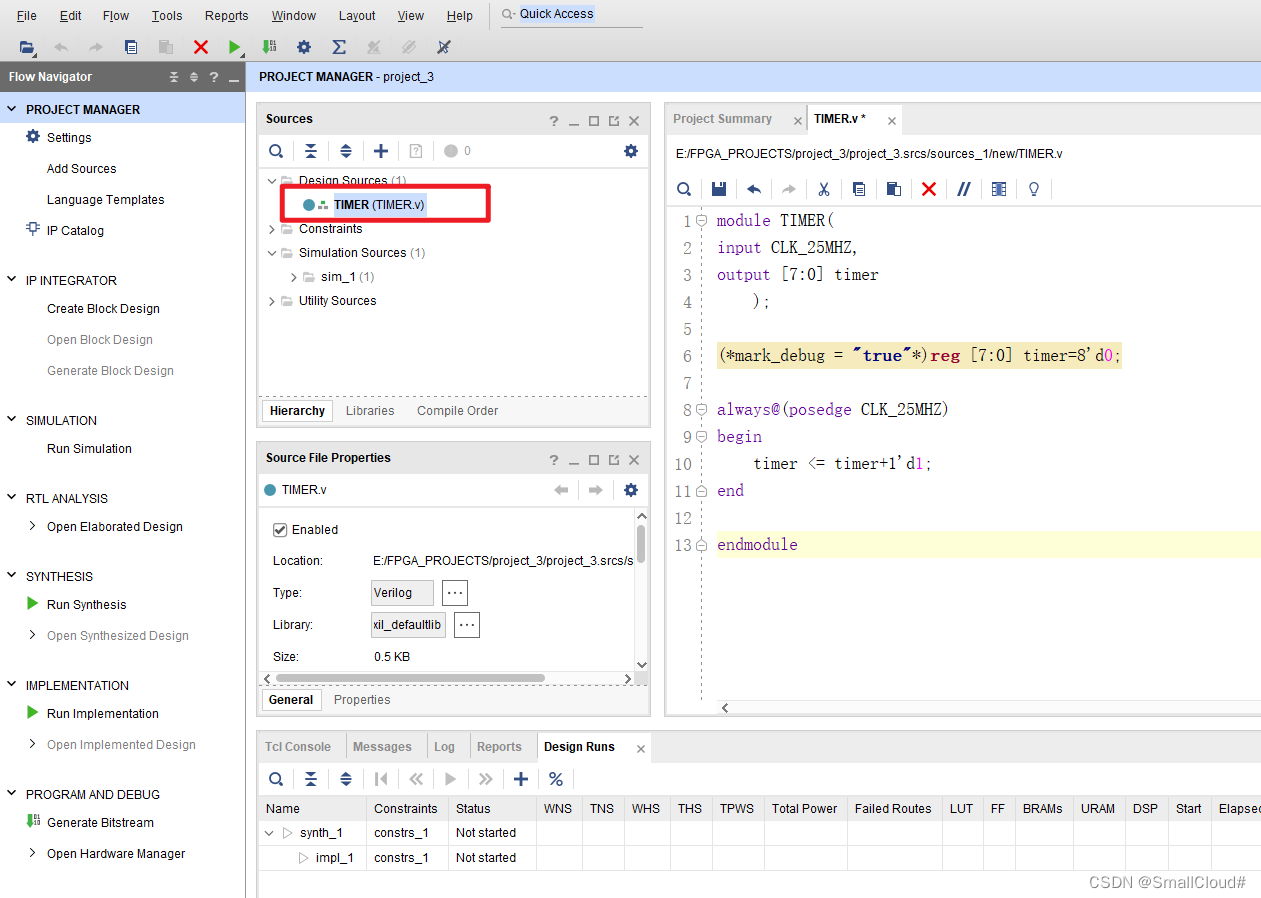
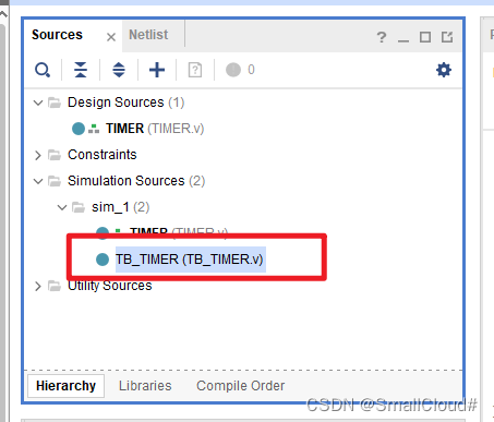
11、 double-click TIMER, Input code save
If the font in the editor is too small, you can change the font size by setting :
13、 Click... On the left Run Synthesis To synthesize , single click OK Then choose Open Synthesized Design, single click OK

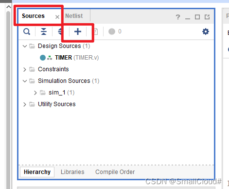
14、 First click Sources Jump back to the source file interface , And then click +, Add simulation file
15、 choice Add or create simulation sources Back click Next

16、 single click Create File Then enter the file name , single click OK, single click Finish

single click OK, single click Yes

17、 Double click the corresponding file name to open the file
18、 Enter the code and save (Ctrl+s)

19、 single click Run Simulation Then choose Run behavioral Simulation, Run the simulation

20、 Enter 1ms Then magnify and observe the waveform

You can see that the rising edge of each clock will accumulate one , The simulation is correct
21、 Close the simulation interface , single click SYNTHESIS Then select I/O Planning

22、 Restrict the pins according to the circuit design , Remember to save when you're done
23、 single click OK, Enter the file name and click OK
24、 Click... In the left column Setup Debug
25、 Click continuously in the pop-up window NEXT
26、 Save the configuration of the signal just monitored , single click OK
27、 single click Generate Bitstream, Create a bitstream , To synthesize 、 Layout and wiring 、 Generate bit file
28、 single click Yes, single click OK
29、 Pop up options View Reports, single click OK
30、 single click Open Hardware Manager
For debugging and simulation ,FPGA Support JTAG Debug mode .JTAG(Joint Test Action Group, Joint test working group ) It's an international standard test protocol (IEEE 1149.1 compatible ), It is mainly used for chip internal test . Most advanced devices now support JTAG agreement , Such as DSP、FPGA Devices, etc . The standard JTAG Interface is 4 Line :TMS、 TCK、TDI、TDO, They are mode selection 、 The clock 、 Data input and data output lines .
- TCK– Test clock input
- TDI– Test data input , Data is passed through TDI Input JTAG mouth
- TDO– Test data output , Data is passed through TDO from JTAG output
- TMS– Test mode selection ,TMS Used to set JTAG The mouth is in a certain test Pattern
- Optional pin TRST– Test reset , Input pin , Low level active
31、 The simulator is connected first FPGA plate JTAG Interface , Then connect the computer USB Interface ,FPGA Access to electricity
32、 single click Open target, Pop up Click Auto Connect
33、 single click Program device
34、 single click Run trigger for this ILA core Button trigger
35、 Enlarge the waveform to view
36、 Close debug window
37、 single click OK,FPGA Power on , Finish debugging
边栏推荐
- Pipnet: face key point detection for natural scenes "pixel in pixel net: directions efficient facial landmark detection in the wild"
- MySQL build websites data table
- Skill list of image processing experts
- Basics - network and server
- Cycle and branch (I)
- 1. Software testing ----- the basic concept of software testing
- What if the test / development programmer gets old? Lingering cruel facts
- 26 points that must be paid attention to for stability test
- My friend took 25koffer as soon as he learned automation test. When will my function test end?
- ERROR: could not extract tar starting at offset 000000000000020980+9231072+2
猜你喜欢

图像识别(六)| 激活函数

Self-supervised learning method to solve the inverse problem of Fokker-Planck Equation

Personally test five efficient and practical ways to get rid of orders, and quickly collect them to help you quickly find high-quality objects!
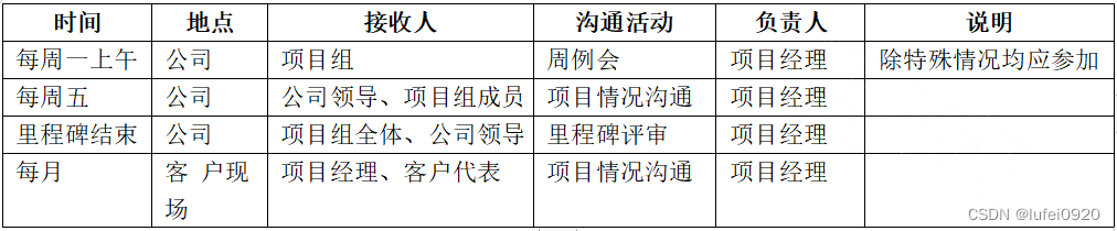
Information System Project Manager - Chapter 10 communication management and stakeholder management examination questions over the years
![[translation] safety. Value of sboms](/img/8b/1ad825e7c9b6a87ca1fea812556f3a.jpg)
[translation] safety. Value of sboms
![[C] Explain language file operation in detail](/img/12/4affa1d3fb3e4ee126e1c1e3872d9b.png)
[C] Explain language file operation in detail
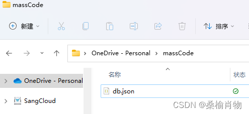
Masscode is an excellent open source code fragment manager
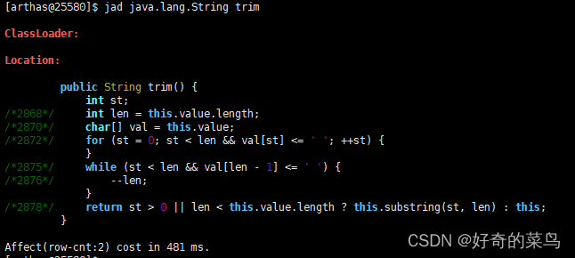
Arthas view the source code of the loaded class (JAD)
![[steering wheel] how to transfer the start command and idea: VM parameters, command line parameters, system parameters, environment variable parameters, main method parameters](/img/97/159d7df5e2d11b129c400d61e3fde6.png)
[steering wheel] how to transfer the start command and idea: VM parameters, command line parameters, system parameters, environment variable parameters, main method parameters
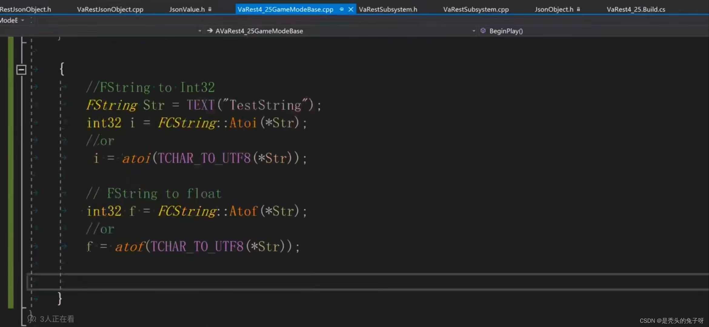
U++ common type conversion and common forms and proxies of lambda
随机推荐
HLS Experiment 1 -- multiplier
Brief introduction and use of NPM link
ERROR: could not extract tar starting at offset 000000000000020980+9231072+2
这种动态规划你见过吗——状态机动态规划之股票问题(上)
Usage of arguments.callee
图像识别(六)| 激活函数
ES6高级-利用原型对象继承方法
ES6高级-利用构造函数继承父类属性
Anti electronic ink screen st7302
AMD64 (x86_64) architecture ABI document:
流形学习、、
U++ common type conversion and common forms and proxies of lambda
Audio and video technology development weekly | 254
Recorded target detection NMS (non maximum suppression)
The LAAS protocol elephant of defi 2.0 is the key to revitalizing the development of defi track
pbootcms上传缩略图尺寸自动缩小变模糊
Application of shift distance and hypothesis
【方向盘】使用IDEA的60+个快捷键分享给你,权为了提效(重构篇)
[pure theory] Yolo v4: optimal speed and accuracy of object detection
Project management: lean management method