当前位置:网站首页>FPGA interview notes (III) -- implementation of handshake signal synchronization in cross clock domain, arbitrary frequency division, binary conversion, RAM memory, original code inversion and complem
FPGA interview notes (III) -- implementation of handshake signal synchronization in cross clock domain, arbitrary frequency division, binary conversion, RAM memory, original code inversion and complem
2022-06-11 06:05:00 【Fighting_ XH】
List of articles
- 1、 Original code 、 Inverse code 、 Complement code
- 2、 Decimal rotation R Hexadecimal encoding and floating-point processing
- 3、 Explanation of terms for various memories
- 4、 Describe the circuit function according to the circuit drawing waveform
- 5、 Any switch 1-8 Frequency division circuit of
- 6、 Consider gray code and state machine
- 7、 Basic methods of data transmission across clock domains
- 8、 Calculation of minimum clock cycle
- 9、 Serial port sends data
- 10、 The concept and basic strategy of temporal constraints
- 11、JK trigger
1、 Original code 、 Inverse code 、 Complement code
1.1、 Original code : Sign bit + Truth value , The highest bit represents the sign bit , Here are four examples , Of a representable range :【-7 , +7】
just 7 :0 111
negative 7: 1 111
1.2、 Inverse code : The inverse of a positive number is itself , The inverse of a negative number is in addition to the sign bit , The rest of you take the opposite . Scope of representation :【-7 , +7】
just 7 :0 111 ( Original code ) —— 0 111( Inverse code )
negative 7: 1 111 ( Original code )—— 1 000( Inverse code )
1.3、 Complement code : The positive complement is the original code , The complement of a negative number is the inverse code +1. Complement value range [-2^ (n-1), 2^( n-1) - 1] , So this range 【-8 , +7】 , Because it doesn't exist -0, So... In the complement 1000 Express -8. So the complement can represent more integers .
just 7 :0 111 ( Original code ) —— 0 111( Inverse code )—— 0 111( Complement code )
negative 7: 1 111 ( Original code )—— 1 000( Inverse code )——1001( Complement code )
1.4、 Why use complements
Although the original code is more intuitive and convenient for decimal conversion, etc , But it is more complicated when adding and subtracting .( such as : Add two numbers , If the sign bits are the same, add , Subtract from different sign bits , When subtracting, you have to compare the absolute value of two numbers , Large number - Small number , Then determine the sign of the final value )
When using complement , The sign bit can also participate in the operation , Without affecting the final result . for example :
-7 + 3 = 1 111( Original code ) + 0011( Original code ) =  1001( Complement code ) + 0101 ( Complement code )= 1100 ( Complement code  )=  1011( Inverse code )= 1100( Original code )= -4
7 + (- 3) =  0111 ( Original code )+ 1 011( Original code ) = 0111( Complement code )+ 1101 ( Complement code ) =  0100( Complement code ) = 0100( Inverse code ) = 0100( Original code ) = 4
-7 + (-1) = 1111( Complement code )+ 1001( Complement code ) = 1000( Complement code ) = -8
1.5 The complement is converted into the original code
The sign bits remain the same , The value is inversed bit by bit , Add... To the bottom 1
Original code 、 Inverse code 、 Complement code
2、 Decimal rotation R Hexadecimal encoding and floating-point processing
Decimal to binary : Integral part + The fractional part
Integral part : Divide R Remainder , Until you can't get rid of ; The fractional part : multiply 2 integer , Until the decimal part of the product is 0
R Convert a decimal number to a decimal number : Expand according to right , Add up —— Relatively simple , I won't repeat
Decimal to octal : First binary , The last three are in a group , The number of digits in the integer part is not enough to fill the left 0, The decimal part is not enough to fill the right 0 Decimal to hexadecimal : In groups of four , The rest are the same .
Give the following example :
Decimal system :20.25 convert
Binary system :10100.01
octal :010 100 . 010
Hexadecimal :0001 0100. 0100
Empathy : Decimal system 46.25 The corresponding binary expression is (101110.01)
In addition, you can also master FPGA The fixed-point processing technology of floating-point numbers in
3、 Explanation of terms for various memories
ROM(Read Only Memory): read-only memory , As the name suggests, you can only read data , It cannot be written , Power off without loss .
RAM(Random Access Memory): Random access memory , Its internal storage data can be taken out and stored at will , At the same time, the reading and writing speed is independent of the position of the stored data in the memory chip .
SRAM(Static Random-Access Memory): Static random access memory , As long as the power supply data can be maintained , Power failure data disappears
DRAM(Dynamic Random Access Memory): Dynamic RAM , How much charge is stored in a capacitor , To represent a bit yes 0 still 1( It can be realized by periodically charging the capacitor Refresh , Then the data will not be lost through constant refresh )
SDRAM(Synchronous Dynamic Random Access Memory): Sync Dynamic RAM , Write and read data synchronously ( Need a clock signal ).
EEPROM(Electrically Erasable Programmable Read-Only Memory): Electrically erasable programmable read only memory ( With the help of a computer program, it is repeatedly erased ).
DDR( Double Data Synchronous Dynamic Random Access Memory): Double rate synchronous dynamic random access memory , Double rate transmission SDRAM, That is, data transmission can be carried out on both the rising and falling edges of the clock .
FLASH(Flash Memory): Flash memory , Nonvolatile solid state storage .( Memory card or U disc )
The following description of memory is correct ( CD ).
A RAM Information will not be lost after power failure , It can be used after the power is turned on
B ROM You can read and write at will
C RAM You can read and write at will
D ROM Information will not be lost after power failure , It can be used after the power is turned on
3.1 FPGA What are the two internal storage resources
FPGA There are two kinds of memory resources in the chip :
1、BLOCK RAM
2、 Distributed RAM( from LUT Configured as internal memory )
BLOCK RAM It is composed of a certain number of fixed size storage blocks , Use BLOCK RAM Resources do not occupy additional logical resources and are fast . but BLOCK RAM The resource consumed is an integer multiple of its block size .
3.2 subject ——SRAM and DRAM Narration
subject 1:—— The second correct

The difference between the two is D and S,S Represents static ,D Show dynamic .
Static is as long as it remains energized , Can store data , In dynamic mode, you need to refresh periodically , Otherwise the data will be lost . therefore 1 4 error .
SRAM Low integration of , Therefore, the power consumption ratio DRAM Big , same-capacity DRAM Memory can be designed for small volumes , however SRAM It takes a lot of volume . A silicon chip of the same area can make a larger capacity DRAM, therefore SRAM The cost of higher .
subject 2:
SRAM Area size is related to those factors ——ABCD
A. Capacity , That is total bit Count
B. Address decoding method
C. No cloth area
D. BIST circuit
subject 3:
( Dajiang 2020 Chip Engineer A volume , The radio )1 individual 16K x 8 Bit memory , The sum of address line and data line is
A、46
B、17
C、48
D、22
analysis :
Address line :16K = 1K * 16 = 1024* 16 = (2 ^10 )*(2^4) = 2^14, That is to say 14 Root address line ;
cable :8 Bit data needs 8 Data line ; Therefore, we need 22 Root line .——D
4、 Describe the circuit function according to the circuit drawing waveform
The following circuit diagram is given , Draw Q0,Q1 as well as Q2 Waveform of , And describe the circuit function ( Pen test )
Topic analysis : You can see that the title is level 3 D trigger , therefore Q0,Q1,Q2 The waveform is the same , Just delay one beat in turn .
about input initial value : Generally, the initial circuit is reset , Therefore, the initial low level at reset 0, Because of input yes Q0 and Q1 And non operation After the value of , therefore input = 1 , Therefore, the input initial value is always high during reset 1.
When reset fails , Start to realize the circuit function .
1、 When analyzing the first input Q0,Q1,Q2 : First clk1 when input = 1 , Therefore, the reset is invalid and clk2 On the rising edge , The output of the first trigger Q0 Receive the last moment input The value of is 1 ,clk3 Rising edge Q1 receive Q0 The value of is 1 ;clk4 Rising edge Q2 receive Q1 The value of is 1.
2、 When analyzing the second input : be based on 1, available clk2 At the time of the input = 0(Q0 and Q1 And non operation results in , Combinatorial logic ), therefore clk3 when Q0 = 0,clk4 when Q1 = 0;clk4 when Q2 = 0;
3、 When analyzing the third input : be based on 2, available clk3 At the time of the input = 0; therefore clk4 when Q0 = 0,clk5 when Q1 = 0;clk6 when Q2 = 0;
By analogy , The following waveform is obtained :
You can see , Output Q2 Protect three cycles in one cycle clk, Therefore, the function realized by this circuit can be called three frequency division .
verilog Code implementation :
 module test(

	input rst_n,
	input clk,
	output reg q2

    );

	wire in1_data;

	reg q0, q1;

	always @(posedge clk or negedge rst_n)
	    if(!rst_n)begin
		     q0 <= 0;
			  q1 <= 0;
			  q2 <= 0;
			  end
		 else begin
		     q0 <= in1_data;
			  q1 <= q0;
			  q2 <= q1;
			  end


	assign in1_data = (~q0) & (~q1);


endmodule
Generated RTL: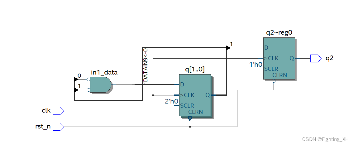
tb Simulation :
`timescale 1ns / 1ps

module test_tb(

    );
	reg clk;
	reg rst_n;

	wire q2;

	initial begin
		clk = 0;
		forever
		#2 clk = ~clk;

	end


	initial begin
		rst_n = 1'b0; #5 rst_n = 1'b1;

	end


	test test_tb(
	.rst_n(rst_n),
	.clk(clk),
	.q2(q2)

	);


endmodule
Waveform :
It can be seen that , It is the same as the waveform obtained from the above analysis .
Therefore, the function of this circuit is three frequency division , Or ternary counter .
5、 Any switch 1-8 Frequency division circuit of
subject 4 It is equivalent to realizing the function of three frequency division , If we want to To achieve arbitrary frequency division circuit How do you do that ?
First, any frequency division circuit is divided into two types : Odd frequency division and even frequency division , Even frequency division can be directly realized by counter , Odd frequency division except counter , It also needs to cooperate with falling edge sampling and combinational logic gate operation .
First of all to FPGA Design , A process is a function definition 、 Design input, etc
1、 Determine the function of any frequency division circuit , Then determine the input and output .
 module test(

	input clk,
	input rst_n,
	input [3:0] div, // Can mean 1-8
	output  clk_out

    );

endmodule
2、 share 8 Two frequency division modes ,1-8 , We can use case Statement .
When the frequency is divided , We set up for eight modes 8 Enable signals to drive respectively (en1,en2……), To simplify , Set up directly reg [7:0] fre_en, Let each bit of it be an enable signal of eight frequency divisions .
// According to the frequency division input value div To determine whether the corresponding frequency division enable signal is valid , such as :div=1, be 1 Frequency division enable signal fre_en[0] It works .

// Define eight frequency division modes
parameter DIV1 = 1,	DIV2 = 2,DIV3 = 3,DIV4 = 4;
parameter DIV5 = 5,	DIV6 = 6,DIV7 = 7,DIV8 = 8;


	always @ (posedge clk or negedge rst_n)
	    if(!rst_n)
		     fre_en <= 8'd00000000; else begin case(div) DIV1: fre_en <= 8'd00000001; //fre_en[0] by 1 Frequency division enable signal
					DIV2: fre_en <= 8'd00000010; //fre_en[1] by 2 Frequency division enable signal  DIV3: fre_en <= 8'd00000100;
					DIV4: fre_en <= 8'd00001000; DIV5: fre_en <= 8'd00010000;
					DIV6: fre_en <= 8'd00100000; DIV7: fre_en <= 8'd01000000;
					DIV8: fre_en <= 8'd10000000; default:fre_en <= 8'd00000000;

		 end
3、 How to realize frequency division in various modes ?
 First 1 Frequency division is equivalent to no frequency division
2 Frequency division can be reversed ~ Realization
 Other frequency division is realized by counting
4、3-8 Counter design
adopt 3-8 The counter is designed to accomplish 3-8 frequency division
//3-8 Counter design
//1、2 Counters are not required for frequency division
	always @(posedge clk or negedge rst_n)
       if(!rst_n)
		     fre_cnt <= 0;
		 else
		     case(1'b1) fre_en[0]: ; //1 frequency division  fre_en[1]: ; //2 frequency division  fre_en[2]:begin //3 frequency division  if(fre_cnt == 4'd2)
					    fre_cnt <= 0;
				   else
					    fre_cnt <= fre_cnt + 1'b1; end fre_en[3]: begin //4 frequency division  if(fre_cnt == 4'd3)
					    fre_cnt <= 0;
				   else
					    fre_cnt <= fre_cnt + 1'b1; end fre_en[4]: begin //5 frequency division  if(fre_cnt == 4'd4)
					    fre_cnt <= 0;
				   else
					    fre_cnt <= fre_cnt + 1'b1; end fre_en[5]: begin //6 frequency division  if(fre_cnt == 4'd5)
					    fre_cnt <= 0;
				   else
					    fre_cnt <= fre_cnt + 1'b1; end fre_en[6]: begin //7 frequency division  if(fre_cnt == 4'd6)
					    fre_cnt <= 0;
				   else
					    fre_cnt <= fre_cnt + 1'b1; end fre_en[7]: begin //8 frequency division  if(fre_cnt == 4'd7)
					    fre_cnt <= 0;
				   else
					    fre_cnt <= fre_cnt + 1'b1;

			  end
			  default:  fre_cnt <= 0;

		 endcase
5、 Design and implementation of frequency division function under eight modes
according to 3、4, We can complete the frequency division function in each mode through the frequency division enable .
// With the frequency division enable signal , And frequency division counting signal , To complete the frequency division function
reg clk_out_r; // Odd frequency division intermediate variable
reg clk_even; // Even frequency division direct output
	always @(posedge clk or negedge rst_n)
       if(!rst_n)
		     clk_even <= 0;
		 else
		     case(1'b1)
			  fre_en[0]: ;   //1 frequency division
			  fre_en[1]: clk_even <= ~ clk_even ; //2 frequency division
			  fre_en[2]:begin //3  frequency division
					if(fre_cnt == 1) // ———— (N-1)/2
				    	 clk_out_r <= ~clk_out_r;
					else if(fre_cnt == 2)
					    clk_out_r <= ~clk_out_r;
					else
					    clk_out_r <= clk_out_r;
				end
			  fre_en[3]:begin //4  frequency division
					if(fre_cnt == 1)
				    	 clk_even <= ~clk_even;
					else if(fre_cnt == 3)
					    clk_even <= ~clk_even;
					else
					    clk_even <= clk_even;
				end
			 fre_en[4]:begin //5  frequency division
					if(fre_cnt == 2)  //———— (N-1)/2
				    	 clk_out_r <= ~clk_out_r;
					else if(fre_cnt == 4)
					    clk_out_r <= ~clk_out_r;
					else
					    clk_out_r <= clk_out_r;
				end

				fre_en[5]: begin // 6 frequency division
					if(fre_cnt == 2)
					    clk_even <= ~clk_even;
					else if(fre_cnt == 5)
					    clk_even <= ~clk_even;
					else
					    clk_even <= clk_even;
				end
				fre_en[6]: begin //7  frequency division
					if(fre_cnt == 3)  //———— (N-1)/2
					    clk_out_r <= ~clk_out_r;
					else if(fre_cnt == 6)
				     	 clk_out_r <= ~clk_out_r;
					else
					    clk_out_r <= clk_out_r;
				end
				fre_en[7]: begin //8  frequency division
					if(fre_cnt == 3)
					    clk_even <= ~clk_even;
					else if(fre_cnt == 7)
					    clk_even <= ~clk_even;
					else
					    clk_even <= clk_even;
					end
			  endcase
6、 Odd frequency division , We can sample the falling edge , Then, the final frequency division result is obtained by performing or operating the signal generated by odd frequency division with the falling edge signal .
// Sampling the falling edge of odd frequency division
// The falling edge of the clock is still detected in the form of a counter
// Write... In the sensitive list , Sampling is only allowed when the clock is on the falling edge

// Falling edge sampling module
	reg clk_nedge;

	always @(negedge clk or negedge rst_n) begin
		if(~rst_n) begin
			clk_nedge <= 0;
		end
		else begin
			case(1'b1)
				fre_en[0]: ;
				fre_en[1]: ;
				fre_en[2]: begin   //3 frequency division
					clk_nedge <= clk_out_r;
				end
				fre_en[3]: ;
				fre_en[4]: begin //5 frequency division
					clk_nedge <= clk_out_r;
				end
				fre_en[5]: ;
				fre_en[6]: begin //7 frequency division
					clk_nedge <= clk_out_r;
				end
				fre_en[7]: ;

			endcase

		end
	end
Frequency division result :
// Generate a division clock
//0 , 2 4 6 8  Frequency division is clk_even
//1 3 5 7  The frequency division signal and the falling edge of the clock shall be calculated
 assign clk_out = ( fre_en[0] | fre_en[1] | fre_en[3] | fre_en[5] | fre_en[7] )? clk_even : (clk_out_r | clk_nedge);
Final verilog Code :
// There are... In the design 1-8 Frequency division of the system , Each frequency division is different , Therefore, we have eight frequency division modes , Different frequency division modes are adopted in each mode

 // Set up 8 An enable signal is used to drive eight modes respectively , To simplify , Set up directly 	reg [7:0] fre_en; Let each bit be used as eight enabling signals of eight frequency divisions


 module test(

	input clk,
	input rst_n,
	input [3:0] div, // Can mean 1-8
	output  clk_out

    );

	 reg [7:0]   fre_en; // Frequency division enable signal


// According to the frequency division input value div To determine whether the corresponding frequency division enable signal is valid , such as :div=1, be 1 Frequency division enable signal fre_en[0] It works .

// Define eight frequency division modes
parameter DIV1 = 1,	DIV2 = 2,DIV3 = 3,DIV4 = 4;
parameter DIV5 = 5,	DIV6 = 6,DIV7 = 7,DIV8 = 8;


	always @ (posedge clk or negedge rst_n)
	    if(!rst_n)
		     fre_en <= 8'd00000000; else begin case(div) DIV1: fre_en <= 8'd00000001; //fre_en[0] by 1 Frequency division enable signal
					DIV2: fre_en <= 8'd00000010; //fre_en[1] by 2 Frequency division enable signal  DIV3: fre_en <= 8'd00000100;
					DIV4: fre_en <= 8'd00001000; DIV5: fre_en <= 8'd00010000;
					DIV6: fre_en <= 8'd00100000; DIV7: fre_en <= 8'd01000000;
					DIV8: fre_en <= 8'd10000000; default:fre_en <= 8'd00000000;
	endcase
		 end

//3-8 Counter design
//1、2 Counters are not required for frequency division
reg [3:0] 	 fre_cnt;
	always @(posedge clk or negedge rst_n)
       if(!rst_n)
		     fre_cnt <= 0;
		 else
		     case(1'b1) // Order priority  fre_en[0]: ; //1 frequency division  fre_en[1]: ; //2 frequency division  fre_en[2]:begin //3 frequency division  if(fre_cnt == 4'd2)
					    fre_cnt <= 0;
				   else
					    fre_cnt <= fre_cnt + 1'b1; end fre_en[3]: begin //4 frequency division  if(fre_cnt == 4'd3)
					    fre_cnt <= 0;
				   else
					    fre_cnt <= fre_cnt + 1'b1; end fre_en[4]: begin //5 frequency division  if(fre_cnt == 4'd4)
					    fre_cnt <= 0;
				   else
					    fre_cnt <= fre_cnt + 1'b1; end fre_en[5]: begin //6 frequency division  if(fre_cnt == 4'd5)
					    fre_cnt <= 0;
				   else
					    fre_cnt <= fre_cnt + 1'b1; end fre_en[6]: begin //7 frequency division  if(fre_cnt == 4'd6)
					    fre_cnt <= 0;
				   else
					    fre_cnt <= fre_cnt + 1'b1; end fre_en[7]: begin //8 frequency division  if(fre_cnt == 4'd7)
					    fre_cnt <= 0;
				   else
					    fre_cnt <= fre_cnt + 1'b1; end default: fre_cnt <= 0; endcase // With the frequency division enable signal , And frequency division counting signal , To complete the frequency division function  reg clk_out_r; // Odd frequency division intermediate variable  reg clk_even; // Even frequency division direct output  always @(posedge clk or negedge rst_n) if(!rst_n) begin clk_even <= 0; clk_out_r <= 0; end else case(1'b1)
			  fre_en[0]: ;   //1 frequency division
			  fre_en[1]: clk_even <= ~ clk_even ; //2 frequency division
			  fre_en[2]:begin //3  frequency division
					if(fre_cnt == 1) // ———— (N-1)/2
				    	 clk_out_r <= ~clk_out_r;
					else if(fre_cnt == 2)
					    clk_out_r <= ~clk_out_r;
					else
					    clk_out_r <= clk_out_r;
				end
			  fre_en[3]:begin //4  frequency division
					if(fre_cnt == 1)
				    	 clk_even <= ~clk_even;
					else if(fre_cnt == 3)
					    clk_even <= ~clk_even;
					else
					    clk_even <= clk_even;
				end
			 fre_en[4]:begin //5  frequency division
					if(fre_cnt == 2)  //———— (N-1)/2
				    	 clk_out_r <= ~clk_out_r;
					else if(fre_cnt == 4)
					    clk_out_r <= ~clk_out_r;
					else
					    clk_out_r <= clk_out_r;
				end

				fre_en[5]: begin // 6 frequency division
					if(fre_cnt == 2)
					    clk_even <= ~clk_even;
					else if(fre_cnt == 5)
					    clk_even <= ~clk_even;
					else
					    clk_even <= clk_even;
				end
				fre_en[6]: begin //7  frequency division
					if(fre_cnt == 3)  //———— (N-1)/2
					    clk_out_r <= ~clk_out_r;
					else if(fre_cnt == 6)
				     	 clk_out_r <= ~clk_out_r;
					else
					    clk_out_r <= clk_out_r;
				end
				fre_en[7]: begin //8  frequency division
					if(fre_cnt == 3)
					    clk_even <= ~clk_even;
					else if(fre_cnt == 7)
					    clk_even <= ~clk_even;
					else
					    clk_even <= clk_even;
					end
			  endcase

// Sampling the falling edge of odd frequency division
// The falling edge of the clock is still detected in the form of a counter
// Write... In the sensitive list , Sampling is only allowed when the clock is on the falling edge

// Falling edge sampling module
	reg clk_nedge;

	always @(negedge clk or negedge rst_n) begin
		if(~rst_n) begin
			clk_nedge <= 0;
		end
		else begin
			case(1'b1)
				fre_en[0]: ;
				fre_en[1]: ;
				fre_en[2]: begin   //3 frequency division
					clk_nedge <= clk_out_r;
				end
				fre_en[3]: ;
				fre_en[4]: begin //5 frequency division
					clk_nedge <= clk_out_r;
				end
				fre_en[5]: ;
				fre_en[6]: begin //7 frequency division
					clk_nedge <= clk_out_r;
				end
				fre_en[7]: ;

			endcase

		end
	end

// Generate a division clock
//0 , 2 4 6 8  Frequency division is clk_even
//1 3 5 7  The frequency division signal and the falling edge of the clock shall be calculated
 assign clk_out = ( fre_en[0] | fre_en[1] | fre_en[3] | fre_en[5] | fre_en[7] )? clk_even : (clk_out_r | clk_nedge);


endmodule
tb Test code :
`timescale 1ns / 1ps `define clock_period 20

module test_tb(


    );

	reg clk;
	reg rst_n;
	reg [3:0] div;
	wire clk_out;

	initial begin
		clk = 0;
		forever
			#2 clk = ~clk;

	end


	initial begin
		rst_n = 0;
		div = 5;
		#15
		rst_n = 1;
		#60
		div = 2;


end

	test u1tb(
	.clk(clk),
	.rst_n(rst_n),
	.div(div),
	.clk_out(clk_out)
	);


endmodule

6、 Consider gray code and state machine
A gray code counter with four bits and sixteen states , The starting value is 1001, after 100 The value after the action of clock pulses is (0011)
- There are two main points in this topic :
1、 If gray code pairs are used 16 States to code
2、100 Which state is it in after clock pulses
- Problem solving
1、 The encoding method of gray code : Any two adjacent codes have only one binary number different . Steps are as follows :
The first way of calculation :
assign gray_code = (bnary >> 1) ^ bnary;
For example : seek 3 Gray code of :
Gray code = (011>> 1 )^ 011 = 001 ^ 011 =010

The second way of calculation :
First step , Change the rightmost bit value ;
The second step , Change the first one from the right to 1 The left bit of the bit ;
For example :
Suppose to produce 4 Bit gray code , Original value bit 0000
First step : Change the rightmost bit value : 0001
The second step : Change the first one from the right to 1 The left bit of the bit : 0011
repeat 1:
The third step : Change the rightmost bit value : 0010
Step four : Change the first one from the right to 1 The left bit of the bit : 0110
repeat 2:
Step five : Change the rightmost bit value : 0111
Step six : Change the first one from the right to 1 The left bit of the bit : 0101
……
In the end we get 4 Bit typical gray code :
2、 After getting gray code , We calculated 100 In which state after the action of clock pulses .
100/16 = 6 more than 4, So after six state cycles , Then add four states . Since the starting value is 1001, therefore 1001 Add... To the status 4, by 0011.
7、 Basic methods of data transmission across clock domains
Which of the following is not the basic method of cross clock domain data transmission ( D ):
A: Use multi-level trigger buffer
B: Use FIFO
C: Using handshake protocol
D: Insert... Into the signal path isolation
Answer key :
A: In data transmission from slow clock domain to fast clock domain , Need to use Two level triggers are synchronized , Eliminate metastable .
B: When multi bit data is transmitted, asynchronous FIFO Handle , Because the synchronized data can only remain stable , But I'm not sure what it is 0 still 1, Therefore, if the multi bit data is buffered by multi-level trigger , There will be garbled code , So we use FIFO.
C: handshake protocol It is often used in the transmission of multi bit data from the slow clock domain to the fast clock domain , Corresponding to the transmission of single bit data from the slow clock domain to the fast clock domain, we often use multi-level trigger synchronization , But the handshake protocol can also be used , It can be determined that the output value at steady state is 0 still 1, So that the data can be transmitted correctly ,
7.1 handshake protocol
The following is the flow of handshake communication :

General steps :
1、 The sending domain puts data into the bus
2、 issue req The request signal is sent to the receiving end , When the receiving end detects that the signal is valid, it can store the data bus
3、 Then send out ack Answer signal , Indicates that the data reading is completed .
4、 Sending domain detected ack After the signal is valid , Undo current req Request signal .
5、 Accepted domain detected req After the request signal is cancelled , It will also ack revoke .
6、 here , Completed a normal handshake communication .
7、 At this time , The next grip communication can be carried out , In turn, cycle ……
Through handshake protocol, we can realize signal synchronization
Handshake agreement RTL as follows :
Including sending domain and receiving domain .
The core part of the :
Send the name of the domain req The request signal is valid , The description tells the receiving domain that the data is ready , Ready to receive .
The accepted domain is based on req The signal will receive data , When the reception is complete , issue ack Answer signal .
When the sending domain detects ack When the signal is high , It indicates that the data has been received and is not required in the request , And then req Set low level , Corresponding ack It also becomes low level .
When the sender req It becomes high level again , Indicates that the next data can be sent ……
Top level module verilog Realization :
// Handshake synchronization design , Including sending domain and receiving domain

module test(
		input  tclk,  // Send clock
		input  rclk , // Receive clock
		input  [31:0] transmit_data ,
		input  reset_tclk,
		input  reset_rclk ,
		input  data_avail ,

		output t_req ,
		output [31:0] t_data ,
		output r_ack
);


// Send module instantiation
transmit u1(
        .tclk(tclk),
        .reset_tclk(reset_tclk),
        .t_req(t_req ),
        .data_avail(data_avail ),
        .transmit_data(transmit_data ),
        .t_data(t_data ),
        .r_ack(r_ack )
		  );


// Receiving module instantiation
receiver u2(
        .rclk(rclk ),
        .reset_rclk(reset_rclk ),
        .t_req(t_req ),
        .t_data(t_data ),
        .r_ack(r_ack )
		  );
endmodule
Sub module : Sending module verilog Realization 
// Sender design
module transmit(

			input tclk,
			input reset_tclk,
			input data_avail,
			input [31:0]transmit_data,
			input r_ack,
			output reg t_req,
			output  reg [31:0]  t_data
);

localparam     IDLE_T = 2'd0; localparam ASSERT_t_req = 2'd1;    // Request signal valid status
localparam     DEASSERT_t_req = 2'd2; // Request signal invalid state  reg [1:0] t_state, t_state_nxt; // At present 、 Next state  reg t_req_nxt; reg [31:0] t_data_nxt; reg r_ack_tclk; // The first segment of the state machine : Status register  [email protected](posedge tclk or negedge reset_tclk)begin if(!reset_tclk) t_state <= IDLE_T; else t_state <= t_state_nxt; end // The second paragraph : Combinatorial logic describes state transitions and outputs  [email protected](*)begin case( t_state) IDLE_T:begin if(data_avail) begin t_req_nxt = 1'b1;
		    t_state_nxt = ASSERT_t_req;
		    t_data_nxt = transmit_data;
		end
		else begin
		   t_req_nxt = 1'b0; t_data_nxt =t_data; t_state_nxt = IDLE_T; end end // Request valid status  ASSERT_t_req:begin if(r_ack_tclk)begin // The response signal is at high level , The request signal is invalid  t_req_nxt = 1'b0;
		     t_state_nxt = DEASSERT_t_req;
		     t_data_nxt = 'd0; end else begin t_req_nxt = 1'b1;
		     t_data_nxt = transmit_data;
			  t_state_nxt = ASSERT_t_req;
		end
	  end

// Request invalid state
  DEASSERT_t_req:begin
   if(!r_ack_tclk)begin   // The high level of the response signal changes to the low level , It means that a handshake is over , At this time, it is judged that the next data is valid ……
       if(data_avail)begin
           t_req_nxt = 1'b1; t_state_nxt = ASSERT_t_req; t_data_nxt = transmit_data; end else begin t_req_nxt = 1'b0;
           t_state_nxt = IDLE_T;
			  t_data_nxt = 'd0; end end end endcase end // The output is delayed by one beat  [email protected](posedge tclk or negedge reset_tclk)begin if(!reset_tclk)begin t_req <= 1'b0;
        t_data <= 32'h00000000; r_ack_tclk <= 1'b0;
 end

 else begin
		  t_req <= t_req_nxt;
		  t_data <= t_data_nxt;
		  r_ack_tclk <= r_ack;    // A reply signal to the receiving domain
 end

end
endmodule
Sub module : Receiving module verilog Realization 
module receiver(

		input rclk,
		input reset_rclk,
		input t_req,
		input[31:0] t_data,
		output reg r_ack


);

		reg r_state,r_state_nxt; // The present state and the secondary state
		reg t_req_rclk;          // Send the request signal from the domain
		reg[31:0] t_data_rclk;
		reg[31:0] t_data_rclk_nxt;
		reg r_ack_nxt;

localparam    IDLE_R     = 1'b0; localparam ASSERT_ACK = 1'b1;


// The first segment of the state machine , Status register

[email protected](posedge rclk or negedge reset_rclk)
 if(!reset_rclk)
	  r_state <= IDLE_R;

 else
	  r_state <= r_state_nxt;


// The second segment of the state machine , Combinatorial logic expresses state transition and output
[email protected](*)begin


 case(r_state)
  IDLE_R:begin
   if(t_req_rclk)begin  // When a valid request signal from the transmission domain is received , Then jump to the reply valid state
		 r_state_nxt = ASSERT_ACK;
		 t_data_rclk_nxt = t_data; // Store the data sent from the sending domain on the receiving domain bus
		 r_ack_nxt = 1'b1; // At this time, the response is high  end else begin r_state_nxt = IDLE_R; t_data_rclk_nxt = t_data_rclk; r_ack_nxt = 1'b0;
	 end
  end

  ASSERT_ACK:begin // Reply valid status
   if(!t_req_rclk)begin // If the request is invalid , The reply signal is also invalid
       r_state_nxt = IDLE_R;
       r_ack_nxt = 1'b0; end else begin r_ack_nxt = 1'b1;
   end
  end

 endcase
end

// The output is delayed by one beat
[email protected](posedge rclk or negedge reset_rclk)begin
 if(!reset_rclk)begin

	  t_data_rclk <= 1'b0; t_req_rclk <= 1'b0;
	  r_ack <= 1'b0;
 end

 else begin
	  t_data_rclk <= t_data_rclk_nxt;
	  t_req_rclk <= t_req;
	  r_ack <= r_ack_nxt;
 end
end

endmodule
tb The test file :
Give two sets of data for verification
`timescale 1ns/1ns
module test_tb ;

		reg tclk ,rclk ;
		reg [31:0] transmit_data ;
		reg reset_tclk ,reset_rclk ;
		reg data_avail ;
		wire t_req ;
		wire [31:0] t_data ;
		wire r_ack ;

parameter CLK_HALF_PERIOD1 = 5;
parameter CLK_HALF_PERIOD2 = 8;
parameter RESET_DELAY = 100;


test u1(
    .tclk (tclk ),
	 .rclk (rclk ),
	 .transmit_data (transmit_data ),
	 .reset_tclk (reset_tclk ),
	 .reset_rclk (reset_rclk ),
	 .data_avail (data_avail ),
	 .t_req (t_req ),
	 .t_data (t_data ),
	 .r_ack (r_ack )
	 );


// Generate clock excitation
initial begin
 tclk  = 0;
 rclk  = 0;
end

always #CLK_HALF_PERIOD1 tclk = ~tclk ;
always #CLK_HALF_PERIOD2 rclk = ~rclk ;

// Generate reset excitation
initial begin
 reset_rclk  = 0;
 reset_tclk  = 0;
 #RESET_DELAY reset_rclk = 1;
 reset_tclk  = 1;
end

// Generate input
initial begin
 #500;
 data_avail  = 1;
 transmit_data  = 32'h57431446; #200; data_avail = 0; #200; data_avail = 1; transmit_data = 32'h77411146;
 #1000;
 $stop;
end


endmodule
The overall simulation waveform is as follows :
We give two sets of data .
Analyze the signal :
When the data is valid ,data_avial = 1, At this high level, according to the reply signal r_ack, Request signal t_req High and low level changes can be realized . When the request signal is high , The receiving domain receives data , therefore t_data The data at the sending end is received at the rising edge of the clock transmit_data, When the request signal is invalid , This indicates that the receiving end cannot receive data , The data is 0.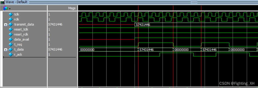
You can also see that when the data is valid , The request signal can change according to the response signal , Low level of simultaneous response signal , The request signal becomes high ;
When the data is invalid , The request response signal is 0, The same receiving domain data is 0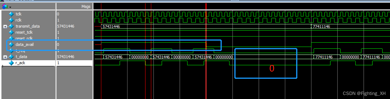
As can be seen from the figure below , Each data reception occurs at the rising edge of the clock in the transmission domain , Therefore, the data is received correctly 
Handshake synchronization signal Of Code reference
8、 Calculation of minimum clock cycle
Formula and analysis of minimum clock cycle
subject :
Tco = 1ns,Tsu = 2ns,Thold = 1ns,Tlogic_max = 4ns, Tlogic_min = 3ns, Jitter = 2ns, Find the minimum clock cycle :
Tmin = Tco + Tlogicmax + Tsu - Tskew + Tjitter = 8ns
From this, the maximum clock frequency can also be calculated :T = 1/ Tmin
9、 Serial port sends data
subject : Simply draw the serial port transmission sequence diagram , Whether the serial port can send valid data bits at one time is determined by 8 Turn into 1024? And explain why , Why can or can not .
When sending through serial port : When idle , The data line is high , Then the start bit ( Low level ), Data bits (8 position ), Stop bit ( High level ).
If the data we want to send now is 01010101, Then the serial port transmission sequence diagram is as follows : Be careful : Start transmission from low bit 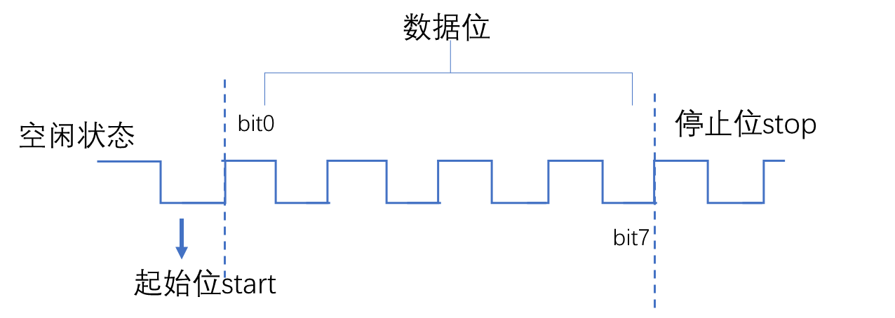
In the serial port data transmission, the serial port sends the significant bit at a time, which is generally 8 position , The transmission is over 8 After bit data , Enter the idle state , And then carry out the next 8-bit data transmission .
Serial port Portland has 9600、115200 etc. , When the baud rate is 115200 when , Serial port clock is required 115200Hz,FPGA The clock cannot produce this baud clock accurately , Therefore, there will be errors in each transmission bit . So if you want to send valid data at one time 1024, That is to say 1024 position , There will be errors, and the more data, the greater the error , May cause sampling errors .
10、 The concept and basic strategy of temporal constraints
Timing constraints mainly include Periodic constraints , Offset constraint , Static timing path constraint Three . By adding timing constraints, the generic cabling tool can adjust the mapping and layout , The design meets the timing requirements
The general strategy of attaching temporal constraints is to attach global constraints first , Rear alignment 、 Special constraints are attached to slow exception paths .
When attaching global constraints, first define all the clocks of the design , The synchronization elements in each clock domain are grouped , Add a periodic constraint to the group , Then on FPGA Input and output PAD Additional offset constraints 、 For all combinatorial logic PAD TO PAD Path additional constraints .
When special constraints are attached , First, the paths between groups are constrained , Then constrain fast 、 Slow exception paths and multi cycle paths , And other special paths .
The role of additional constraints
1: Reduced logic and wiring delays , So as to improve the working frequency of the design circuit ;
2: Get the correct timing analysis report ;( The static timing analysis tool takes constraints as the criteria to judge whether the timing meets the design requirements , Therefore, designers are required to input constraints correctly , So that the static timing analysis tool can output the correct timing report )
3: Appoint FPGA Electrical standards and pin locations for .
11、JK trigger
The following circuit is given , Write the driving equation and draw the waveform , Describe its function .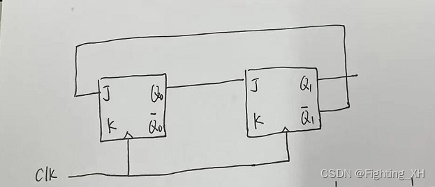
Driving equation :
Waveform :
function : The descriptive duty cycle is 1/3 Frequency division signal .
Reference resources NingHeChuan A collection of interview questions from the boss
边栏推荐
- Servlet
- Print sparse arrays and restore
- Dichotomy find template
- “All in ONE”一个平台解决所有需求,运维监控3.0时代已来
- Getting started with kotlin
- Summarize the five most common BlockingQueue features
- [daily exercise] 217 Duplicate element exists
- Jsonobject jsonarray for parsing
- 我们真的需要会议耳机吗?
- Continuous update of ansible learning
猜你喜欢

Login and registration based on servlet, JSP and MySQL
![[metadata]linkedin datahub](/img/6a/247ee77dfc219d26651e5d93b04c98.png)
[metadata]linkedin datahub

More than 20 cloud collaboration functions, 3 minutes to talk through the enterprise's data security experience

Jsonobject jsonarray for parsing
Error reporting injection of SQL injection

Sign for this "plug-in" before returning home for the new year

Install Oracle Database

What do you need to know about Amazon evaluation?

verilog实现双目摄像头图像数据采集并modelsim仿真,最终matlab进行图像显示
Installing and using sublist3r in Kali
随机推荐
Set the IP address using batch
Cenos7 builds redis-3.2.9 and integrates jedis
Basic usage of MySQL
數組部分方法
Use of constructors
What happened to the young man who loved to write code -- approaching the "Yao Guang young man" of Huawei cloud
The artistic director and production designer of Disney's Mandalorian revealed the virtual scene production behind it
Basic use of BufferedReader and bufferedwriter
Yonghong Bi product experience (I) data source module
箭头函数的this指向
Deployment of Flink
做亚马逊测评要了解的知识点有哪些?
YOLOv5的Tricks | 【Trick8】图片采样策略——按数据集各类别权重采样
Matlab实现均值滤波与FPGA进行对比,并采用modelsim波形仿真
Slide the receleview horizontally to the far right to listen to the page loading function
call和apply和bind的区别
ThymeleafEngine模板引擎
修复【无 Internet, 安全】问题
Informatica: six steps of data quality management
Warmly celebrate that yeyanxiu, senior consultant of Longzhi, won the title of "atlassian Certified Expert"