当前位置:网站首页>Esp32 series (3): GPIO learning (take simple GPIO input and output, ADC, DAC as examples)
Esp32 series (3): GPIO learning (take simple GPIO input and output, ADC, DAC as examples)
2022-07-03 03:54:00 【w0shishabi】
Catalog
1 ESP32 GPIO Basic concepts
ESP32 The chip has 34 Physics GPIO pad(GPIO PAD Number :0-19, 21-23, 25-27, 32-39. among GPIO 34-39 Only used as input pins , Others can be used as both input and output pins .). Every pad Can be used as a general purpose IO, Or connect an internal peripheral signal .
IO_MUX、RTC IO_MUX and GPIO The switching matrix is used to transmit signals from peripherals to GPIO pad. These modules together make up the chip's IO control
system .

- IO_MUX choice GPIO pad Configure to GPIO( Connect with the exchange matrix ) Or direct connection ( Better high frequency digital characteristics , For high-speed signals )
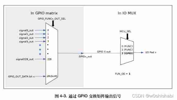
- GPIO Commutative matrix Conduct 【 Peripheral input and output 】 And 【pad The signal 】 Full exchange between . In fact, it's the end pad Selection of input and output signals .
- RTC IO_MUX control GPIO pad Low power consumption and analog function .
1.1 adopt GPIO Peripheral input of exchange matrix
34 individual GPIO(X: 0-19,21-23,25-27,32-39)
obtain
Index number of peripheral input signal (Y: 0-18,23-36,39-58,61-90,95-124,140-155,164-181,190-195,198-206)

a key : Send a peripheral signal Y Bind to something GPIO pad X The configuration process of is :
- stay GPIO Configure Peripheral signals Y Of
GPIO_FUNCy_IN_SEL_CFGregister :- Set up
GPIO_FUNCy_IN_SELThe field is to be readGPIO pad XValue . Clear other GPIO pad Other fields for .
- Set up
- stay GPIO Configure GPIO pad X Of
GPIO_FUNCx_OUT_SEL_CFGregister 、 Zero clearingGPIO_ENABLE_DATA[x]Field :- To force the output state of the pin to always be determined by
GPIO_ENABLE_DATA[x]Field decision , WillGPIO_FUNCx_OUT_SEL_CFGThe register ofGPIO_FUNCx_OEN_SELThe field position is 1. GPIO_ENABLE_DATA[x]Field inGPIO_ENABLE_REG(GPIOs 0-31) orGPIO_ENABLE1_REG(GPIOs 32-39) in , Clearing this bit can close GPIO pad Output .
- To force the output state of the pin to always be determined by
- To configure IO_MUX Register to select GPIO Commutative matrix . To configure GPIO pad X Of
IO_MUX_x_REGThe process is as follows :- Set function fields (MCU_SEL) by GPIO X Of IO_MUX function ( Of all pins Function 2, Values for 2).
- Set up FUN_IE Enable input .
- To set or clear FUN_WPU and FUN_WPD position , Enable or close the internal pull-up / Pull down resistor .
explain :
- The same input pad Multiple internal can be bound at the same time input_signals.
- Set up GPIO_FUNCy_IN_INV_SEL You can invert the input signal .
- There is no need to bind the input signal to a pad It can also make the peripheral read the input value of constant low or constant high level . The implementation method is to select a specific
GPIO_FUNCy_IN_SEL Enter a value instead of a GPIO Serial number :- When GPIO_FUNCy_IN_SEL yes 0x30 when , input_signal_x Always be 0.
- When GPIO_FUNCy_IN_SEL yes 0x38 when , input_signal_x Always be 1.
Example : hold RMT Peripheral channel 0 The input signal of RMT_SIG_IN0_IDX( Signal index number 83) Bound to the GPIO15, Follow these steps ( Please note that GPIO15 It's also called MTDO Pin ):
- take GPIO_FUNC83_IN_SEL_CFG The register of GPIO_FUNC83_IN_SEL Field set to 15.
- Because this signal is a pure input signal , Set up GPIO_FUNC15_OUT_SEL_CFG_REG In register GPIO_FUNC15_OEN_SEL position .
- Zero clearing GPIO_ENABLE_REG The register of bit 15(GPIO_ENABLE_DATA[15] Field ).
- To configure IO_MUX_GPIO15 The register of MCU_SEL Field is 2 (GPIO function), Simultaneous setting FUN_IE( Enable input mode ).
ordinary GOIO Input :
- GPIO_IN_REG/GPIO_IN1_REG Registers store each GPIO pad The input value of .
- arbitrarily GPIO pin The input value of can be read at any time without configuring a peripheral signal GPIO Commutative matrix . But it needs to be for pad X Of
IO_MUX_x_REG Register configuration FUN_IE Bits to enable input .
1.2 adopt GPIO Peripheral output of exchange matrix
28 individual GPIO (X: 0-19, 21-23, 25-27, 32-33)
obtain
Peripheral signals (Y: 0-18, 23-37, 61-121,140-215, 224-228)
a key : Output peripheral signals Y To a certain GPIO pad X The steps are :
- stay GPIO Configure in the exchange matrix GPIO X Of GPIO_FUNCx_OUT_SEL_CFG Registers and GPIO_ENABLE_DATA[x] Field :
- Set up GPIO_FUNCx_OUT_SEL_CFG The register of GPIO_FUNCx_OUT_SEL Field is peripheral output signal Y The index number of (Y).
- To force the signal to the output mode , take GPIO pad X Of GPIO_FUNCx_OUT_SEL_CFG The register of GPIO_FUNCx_OEN_SEL Set up , And will GPIO_ENABLE_REG The register of GPIO_ENABLE_DATA[x] Field set . perhaps , take GPIO_FUNCx_OEN_SEL Zero clearing , At this time, the output enable signal is determined by the internal logic function .
- GPIO_ENABLE_DATA[x] Field in GPIO_ENABLE_REG (GPIOs 0-31) or GPIO_ENABLE1_REG (GPIOs32-39) in , Clearing this bit can turn off GPIO pad Output .
- To choose to output in open drain mode , You can set GPIO X Of GPIO_PINx In register GPIO_PINx_PAD_DRIVER position .
- To configure IO_MUX Register to select GPIO Commutative matrix . To configure GPIO pad X Of IO_MUX_x_REG The process is as follows :
- Set function fields (MCU_SEL) by GPIO X Of IO_MUX function ( Of all pins Function 2, Values for 2).
- Set up FUN_DRV The field is a specific output intensity value (0-3), The bigger the value is. , The stronger the output driving ability .
- In open drain mode , By setting / Zero clearing FUN_WPU and FUN_WPD Enable or close pull-up / Pull down resistor .
explain :
- The output signal of a peripheral can be transmitted from multiple at the same time pad Output .
- Set up GPIO_FUNCx_OUT_INV_SEL You can invert the output signal .
ordinary GOIO Output :
- GPIO Commutative matrices can also be used for simple GPIO Output . Set up GPIO_OUT_DATA The value of a bit in the register can be written to the corresponding GPIO pad.
- To achieve a pad Of GPIO Output , Set up GPIO Commutative matrix GPIO_FUNCx_OUT_SEL Registers are specific peripheral index values 256(0x100).
1.3 direct I/O
It can be seen from the previous overall input and output structure block diagram ,IO_MUX There are also some direct I/O The signal . Fast signals such as Ethernet 、 SDIO、 SPI、 JTAG、 UART Wait a minute GPIO Exchange matrices to achieve better high-frequency digital characteristics .
1.4 RTC IO_MUX Input and output
18 individual GPIO Pins have low power consumption ( low power consumption RTC) Performance and simulation functions , These functions do not go through IO_MUX and GPIO Commutative matrix , But use RTC_MUX take I/O Point to RTC Subsystem .
When these pins are configured as RTC GPIO Pin , As an output pin, the chip can still be in Deep-sleep Keep output in sleep mode
The level value or when used as an input pin can change the chip from Deep-sleep Wake up in the .
2 Code implementation
2.1 Simple GPIO Input / output implementation
The actual realization ,ESP-IDF The official document will GPIO The settings of are encapsulated into functions :gpio_config.
@path: gpio.h
@brief: GPIO General configuration function , To configure  GPIO  The pattern of , Pull up , The drop-down , interrupt
@param:  A pointer to a ** GPIO  Configuration structure ** The pointer to  pGPIOConfig
@return: ESP_OK: success ;ESP_ERR_INVALID_ARG: Parameter error

esp_err_t gpio_config(const gpio_config_t *pGPIOConfig);
GPIO Configuration structure :
/**
 * @brief Configuration parameters of GPIO pad for gpio_config function
 */
typedef struct {
    uint64_t pin_bit_mask;          /*!< GPIO pin: set with bit mask, each bit maps to a GPIO */
    gpio_mode_t mode;               /*!< GPIO mode: set input/output mode                     */
    gpio_pullup_t pull_up_en;       /*!< GPIO pull-up                                         */
    gpio_pulldown_t pull_down_en;   /*!< GPIO pull-down                                       */
    gpio_int_type_t intr_type;      /*!< GPIO interrupt type                                  */
} gpio_config_t;
To configure GPIO1 For export 、GPIO3 Take input as an example . The code is :
#include <stdio.h>
#include <string.h>
#include <stdlib.h>
#include "driver/gpio.h"
#include "freertos/FreeRTOS.h" //portTICK_RATE_MS
#include "freertos/task.h" //vTaskDelay
/**
 * Brief:
 *  Basic GPIO Input output learning
 *
 * GPIO status:
 * GPIO1: output
 * GPIO3:  input
 *
 * Test:
 * Connect GPIO1 with GPIO3
 * Generate pulses on GPIO3, that connect to GPIO3
 *
 */
#define GPIO_2   2
#define GPIO_4   4

void app_main(void)
{
    // GPIO1
    gpio_config_t io_conf = {};                 // The new configuration GPIO pad Of gpio_config Structure of functional parameters
    io_conf.pin_bit_mask = (1ULL << GPIO_2);    // Set up GPIO2 The mask of is 1
    io_conf.mode = GPIO_MODE_OUTPUT;            // Set up GPIO1  For output mode
    io_conf.pull_up_en = 0;                     // Don't pull up
    io_conf.pull_down_en = 0;                   // No pull down
    io_conf.intr_type = 0;                      // Ban GPIO2 interrupt
    esp_err_t result;
    result = gpio_config(&io_conf);             // To configure GPIO2
    if (result == ESP_OK)
        printf("gpio2_config succeed \n");
    else
        printf("gpio2_config failed \n");

    // GPIO3
    io_conf.pin_bit_mask = (1ULL << GPIO_4);    // Set up GPIO3 The mask of is 1
    io_conf.mode = GPIO_MODE_INPUT;             // Set up GPIO3  Is the input mode
    result = gpio_config(&io_conf);             // To configure GPIO3
    if (result == ESP_OK)
        printf("gpio4_config succeed \n");
    else
        printf("gpio4_config failed \n");

    int cnt = 0;
    int value = 0;
    while(1)
    {
        cnt++;
        vTaskDelay(1000 / portTICK_RATE_MS);
        gpio_set_level(GPIO_2, cnt % 2);
        printf("GPIO_2_output: %d\n", cnt % 2);
        value = gpio_get_level(GPIO_4);
        printf("GPIO_4_input: %d\n", value);
    }
}
Will develop the GPIO2 And GPIO4 come together 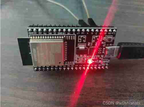
Running results :
2.2 RTC GPIO Input / output implementation
With DAC1 adopt GPIO25 Output 、ADC1 adopt GPIO33 Input as an example .
First, find Le Xin 《esp32 Technical reference manual 》 Of 4.10 Chapter found ADC And DAC Pin mapping of :

You can see DAC_1 Corresponding GPIO25, ADC1_CH5 Corresponding GPIO33 .
For this kind of peripheral input and output , The official peripheral driver file gives the relevant configuration functions , It's also very convenient for us to use , Here is the current dac、adc Application, for example , Introduce the related functions :
- esp_adc_cal_check_efuse
Check whether the current reference voltage is fused to the corresponding position . - adc1_config_width
Set up ADC1 Acquisition bit width - adc1_config_channel_atten
To configure ADC1 The passage of , That is, the corresponding GPIO . And the attenuation of this channel . - esp_adc_cal_characterize
Use the input parameters to configure ADC - esp_adc_cal_raw_to_voltage
According to the sampling value and adc Calculate the voltage value according to the configuration characteristics of .
so , With the official drive , It can eliminate the complicated register configuration process . except ad and da, Other peripherals are also convenient to use .
Test code :
#include <stdio.h>
#include <stdlib.h>
#include "freertos/FreeRTOS.h"
#include "freertos/task.h"
#include "esp_adc_cal.h" //esp_adc_cal_check_efuse
#include "driver/adc.h"
#include "driver/dac.h"
#define DEFAULT_VREF 1100 // Reference voltage
#define NO_OF_SAMPLES 64 // Number of samples
#define AMP_DAC 255 // DAC Output amplitude
static const adc_unit_t unit = ADC_UNIT_1; // ADC1
static const adc_channel_t channel = ADC_CHANNEL_5; // ADC1 GPIO33
static const adc_bits_width_t width = ADC_WIDTH_BIT_12; // ESP32 Integrate 12-bit SAR ADC
static const adc_atten_t atten = ADC_ATTEN_DB_11; // attenuation 11 dB (3.55 x)
static esp_adc_cal_characteristics_t *adc_chars; // ADC Structural storage characteristics
static const dac_channel_t dac_chan = DAC_CHANNEL_1;
void app_main(void)
{
//Check if TP is burned into eFuse
if (esp_adc_cal_check_efuse(ESP_ADC_CAL_VAL_EFUSE_TP) == ESP_OK) {
printf("eFuse Two Point: Supported\n");
} else {
printf("eFuse Two Point: NOT supported\n");
}
//Check Vref is burned into eFuse
if (esp_adc_cal_check_efuse(ESP_ADC_CAL_VAL_EFUSE_VREF) == ESP_OK) {
printf("eFuse Vref: Supported\n");
} else {
printf("eFuse Vref: NOT supported\n");
}
// Configure bit width
if (adc1_config_width(width) == ESP_OK ) {
printf("adc1_config_width: ESP_OK\n");
} else {
printf("adc1_config_width: ESP_ERR_INVALID_ARG\n");
}
// stay ADC1 Set the attenuation of a specific channel on , And configure its associated GPIO RTC_MUX.
if (adc1_config_channel_atten(channel, atten) == ESP_OK ) {
printf("adc1_config_channel_atten: ESP_OK\n");
} else {
printf("adc1_config_channel_atten: ESP_ERR_INVALID_ARG\n");
}
// structure ADC Structural storage characteristics
adc_chars = calloc(1, sizeof(esp_adc_cal_characteristics_t)); // Allocate a memory block .
esp_adc_cal_value_t val_type = esp_adc_cal_characterize(unit, atten, width, DEFAULT_VREF, adc_chars);
// Can make DAC Output
if (dac_output_enable(dac_chan) == ESP_OK ) {
printf("dac_output_enable: ESP_OK\n");
} else {
printf("dac_output_enable: ESP_ERR_INVALID_ARG\n");
}
int cnt = 0;
while(1)
{
uint32_t adc_reading = 0;
cnt++;
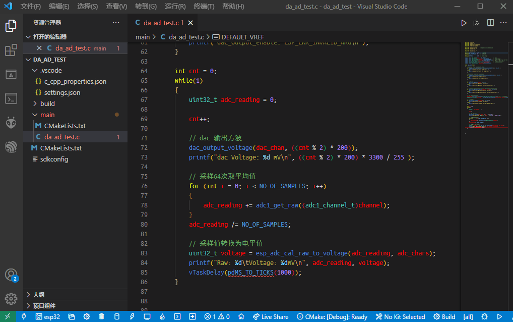
// dac Output square wave
dac_output_voltage(dac_chan, ((cnt % 2) * 200));
printf("dac Voltage: %d mV\n", ((cnt % 2) * 200) * 3300 / 255 );
// sampling 64 Take the average of times
for (int i = 0; i < NO_OF_SAMPLES; i++)
{
adc_reading += adc1_get_raw((adc1_channel_t)channel);
}
adc_reading /= NO_OF_SAMPLES;
// The sampling value is converted to the level value
uint32_t voltage = esp_adc_cal_raw_to_voltage(adc_reading, adc_chars);
printf("Raw: %d\tVoltage: %dmV\n", adc_reading, voltage);
vTaskDelay(pdMS_TO_TICKS(1000));
}
}
Connect GPIO25 And GPIO33.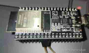
Debugging results :
It is worth noting that ,ESP32 ADC Different attenuation values have corresponding input voltage support range , So here 0mV Uncertainty is normal .
| Attenuation configuration value | attenuation (dB) | Range of input voltage supported (mV) |
|---|---|---|
| ADC_ATTEN_DB_0 | 0 | 100 ~ 950 |
| ADC_ATTEN_DB_2_5 | 2.5 | 100 ~ 1250 |
| ADC_ATTEN_DB_6 | 6 | 150 ~ 1750 |
| ADC_ATTEN_DB_11 | 11 | 150 ~ 2450 |
边栏推荐
- Separable bonds and convertible bonds
- 递归:一维链表和数组
- shardingsphere动态数据源
- Without sxid, suid & sgid will be in danger- Shangwen network xUP Nange
- [mathematical logic] propositional logic (propositional and connective review | propositional formula | connective priority | truth table satisfiable contradiction tautology)
- Ffmpeg download and installation tutorial and introduction
- Use of sigaction
- Makefile demo
- Filter
- Arlo's thinking about himself
猜你喜欢
numpy之 警告VisibleDeprecationWarning: Creating an ndarray from ragged nested sequences

2022 tea master (intermediate) examination questions and analysis and tea master (intermediate) practical examination video

Ffmpeg recording screen and screenshot

ffmpeg之 一张/多张图片合成视频

没有sXid,suid&sgid将进入险境!-尚文网络xUP楠哥
What can learning pytorch do?

在 .NET 6 项目中使用 Startup.cs
Leetcode: dynamic planning template
简易版 微信小程序开发之页面跳转、数据绑定、获取用户信息、获取用户位置信息

2022 polymerization process examination questions and polymerization process examination skills
随机推荐
Dynamic programming: longest common substring and longest common subsequence
ffmpeg之 一张/多张图片合成视频
Read a paper_ ChineseBert
Introduction à mongodb
释放数据力量的Ceph-尚文网络xUP楠哥
[mathematical logic] propositional logic (equivalent calculus | idempotent law | exchange law | combination law | distribution law | De Morgan law | absorption rate | zero law | identity | exclusion l
The latest analysis of the main principals of hazardous chemical business units in 2022 and the simulated examination questions of the main principals of hazardous chemical business units
[mathematical logic] propositional logic (propositional and connective review | propositional formula | connective priority | truth table satisfiable contradiction tautology)
C语言HashTable/HashSet库汇总
Makefile demo
QSAR model establishment script based on pytoch and rdkit
vim 的实用操作
TCP/IP模型中的重磅嘉宾TCP--尚文网络奎哥
2022-07-02:以下go语言代码输出什么?A:编译错误;B:Panic;C:NaN。 package main import “fmt“ func main() { var a =
学会pytorch能干什么?
FileZilla Client下載安裝
IPv6过渡技术-6to4手工隧道配置实验--尚文网络奎哥
2022 P cylinder filling examination content and P cylinder filling practice examination video
[DRM] simple analysis of DRM bridge driver call process
没有sXid,suid&sgid将进入险境!-尚文网络xUP楠哥