当前位置:网站首页>Yilingsi T35 FPGA drives LVDS display screen
Yilingsi T35 FPGA drives LVDS display screen
2022-07-27 03:17:00 【ltqshs】
Yilingsi FPGA, Natural fit MIPI/LVDS And so on , Plus a hard core DDR3 controller , It's perfect .
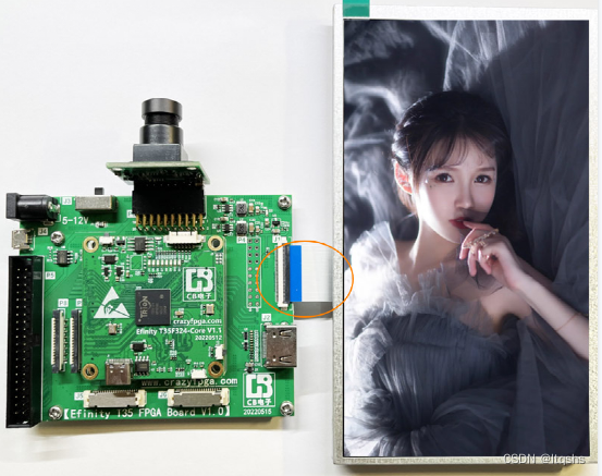
T35F324 Development board support LVDS LCD Display and HDMI Show , The specific block diagram is as follows . here , I will spend some time , Tell me about Trion series FPGA T35 Of LVDS TX Hard IP How to use , And the actual combat drives my design 1024*600 Of 7 " LVDS The screen .
1. Hardware introduction
As shown in the figure below , by 1024*600 LVDS LCD Interface , Here directly with FPGA Of LVDS IO Docking drive , It's related to Bank Used 3.3V level . Because I am LCD All power drives have been handled on the side of the drive board , So user interface driver , Only need to PWM And LVDS Data is enough .

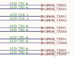
among LVDS by 1 For differential clock ,4 For differential data lines , Look up LCD manual ( Group creation ), The relevant driver protocols are as follows (8bit DE Pattern , The clock adopts 3:4 Duty cycle )
in addition ,1024*600 Driving timing of , As shown below . Here the clock range is 40.8~67.2MHz, And the timing is the same as VGA Timing Exactly the same as . I have introduced in detail how to drive VGA Monitor , Here it is LVDS Previous RGB sequential , It's exactly the same .

So our whole Pipeline It should be :lcd_driver <–> lcd_display --> LVDS Interface
2.Trion FPGA LVDS principle

open Efinity Software , Click on Help-Document, stay Interface Designer Find LVDS Interface, Inquire about Trion series FPGA Of LVDS Interface, As shown in the figure below :

so LVDS Is the hard core , And support 800MHz LVDS rate , compatible 2:1 ~ 8:1, also FPGA The chip has been integrated 100R Terminal resistance , As shown below :

in addition , If LVDS bank be used for GPIO, It is required to be adjacent 2 Yes unassigned LVDS pins, Otherwise, the software will report an error

next , With LVDS TX For example , Let's open the relevant section , See the block diagram given in the document :

here , from PLL produce fastclk And slowclk, supply Serializer, Then output serial data . With n=7 For example ,help The following sequence diagram is given , Namely, in accordance with the 3:4, Output 7bit The data of .

in addition , It is important to note that in Using the Trion LVDS Block in , so fastclk0 And slowclk The relationship between . First fastclk Namely serial clock, slowclk Namely parallel cock; secondly , stay Trion series FPGA in ,fastclk=slowclkn/2, So when n=7 when ,fastclk=3.5slowclk.

3.LVDS TX Design process
Analysis finished Trion FPGA Of LVDS TX characteristic , We have rice to cook , Direct knife , as follows :
1) First ,File→Create Project, Create a project , Select the corresponding device

2) Then add the existing code (99.9% Of people are transplant , I won't start studying in China )

3) then , open Interface, Configure clock 、 Pin 、PLL, And phase locked loop

a.Create Block establish IO, Include clk、lcd_pwm Control signals 
If this is GPIO, Select input or output ; If it is clk, What kind of clock do you have , As shown below :
Here we define pll_clkin, The hardware is connected to PLL_CLKIN Pin , It cannot be used for other purposes , as follows :

b. Then configure the pin , Operate against the schematic diagram , This will show Resource, As shown below :

c. Then set PLL, stay PLL It's about Create Block, establish tx_pll as follows . Here we need to choose PLL_BR0, Corresponding clk Input pin , Hardware fixation is GPIOR_138.

d. open Automated Clock Calculation, Configure the clock input as 24MHz, Output slow clock 48MHz, Fast clock = Slow clock *3.5=168MHz(lvds=7bit), And a fast clock needs 90 degree phase, as well as txpll_locked,GUI The configuration is as follows ( Consistent with the previous analysis ):
e. Last , To configure LVDS IO, As shown below , Note that LVDS Resource The choice of , as well as Serialization Width=7, And choose tx_fastclk Name , The software will automatically according to this Name Conduct wire:
there LVDS TX perhaps CLK, It must be consistent with the allocation in the hardware schematic , as follows :
picture
f. Last ,Generate Efinity Constraint file , If there is an error, it will be reported at this time , Such as no 90°, Or the magnification is wrong ,IO The distribution is not equal . After this step is completed, the constraint file of the project is generated , Including the top shell .
Generated files , Can be found in Result Medium Interface see , as follows , Special attention sdc And template.v
4)LCD_LVDS_Test_1024600.v Modification of top-level code
In the last step , Software helps us generate top-level template.v, As shown below :

so PLL The output clock of , It is directly used as the input clock of our logic ; in addition ,LVDS We only need to input the configured 7bit Serial clock and data , Besides, we don't need to instantiate PLL、LVDS IP etc. . This first meeting , It's really very strange .
a. So , Our top-level interface becomes like this . Here, the pixel clock is naturally a slow clock ,clk and fast The clock doesn't need to be commented out by us :

b. Normalization rgb lcd Driver code , as follows :
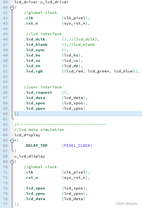
c. take rgb And de Data to lvds port, There's a bit of a hole here , At first, I didn't study timing , as follows :
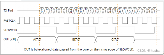
here 7bit Parallel to serial transmission , The first thing to send is lsb, Then it is msb, therefore rgb The driver code needs to be changed , The operation is as follows ( At first, I took it for granted that it was msb, Wasted a lot of precious time ):
5) Last , stay dashboard Double click the icon , Perform a series of compilation 、 comprehensive 、 Layout and wiring , And finally generate the target bit file .

About the resources occupied by the design , It can be on the left Result View in , As shown below , Occupied a PLL,5 individual LVDS:

6) On board verification , open Programmer, choice bit file , Download to FPGA after , Finally, it lights up LVDS The screen , Everything is difficult at the beginning , as follows :

4.Trion FPGA LVDS summary
In conclusion , Yilingsi Trion FPGA Of LVDS TX IP Relevant precautions :
1) First fastclk = n/2 * slowclk;
2) Second, we must remember fastclk Yes 90deg The aspect of
3) Moreover, serial data is sent first LSB, Reissue MSB Of .
4) Last LVDS TX Hard IP After configuration , Use directly at the top of the code , There is no need to instantiate .
Copyright notice , This article is from the Internet :《 Yilingsi T35 FPGA drive LVDS display 》.
边栏推荐
- [dynamic planning medium] leetcode 198. looting 740. delete and get points
- SAFE-ARC/WARNER电源维修XENON氙灯电源维修分析
- 五、MFC视图窗口和文档
- Worth more than 100 million! The 86 version of "red boy" refuses to be a Daocheng Xueba. He is already a doctor of the Chinese Academy of Sciences and has 52 companies under his name
- Hcip day 14 notes
- Portraiture5全新升级版磨皮滤镜插件神器
- Best practices of opentelemetry in service grid architecture
- CAS deployment and successful login jump address
- 阿里云技术专家杨泽强:弹性计算云上可观测能力的构建
- Post responsibilities of safety officer and environmental protection officer
猜你喜欢


![Analysis of [paper] pointlanenet papers](/img/f6/8001be4f90fe15100e0295de02491f.png)


随机推荐
cocos小游戏实战-05-NPC与角色攻击逻辑
Baidu cloud face recognition
易灵思T35 FPGA驱动LVDS显示屏
次轮Okaleido Tiger即将登录Binance NFT,引发社区热议
软件测试面试常见问题及答案(发散思维、接口、性能、概念、)
优炫数据库集群如何唯一标识一条用户SQL
Integrated water conservancy video monitoring station telemetry terminal video image water level water quality water quantity flow velocity monitoring
Abbkine AbFluor 488 细胞凋亡检测试剂盒特点及实验建议
数据湖(二十):Flink兼容Iceberg目前不足和Iceberg与Hudi对比
[dynamic planning medium] leetcode 198. looting 740. delete and get points
Acwing 2074. Countdown simulation
Social wechat applet of fanzhihu forum community
阿里云技术专家杨泽强:弹性计算云上可观测能力的构建
最大连续子序列(DAY 77)
二叉树(北京邮电大学机试题)(DAY 85)
毕业2年转行软件测试获得12K+,不考研月薪过万的梦想实现了
Inftnews | "traffic + experience" white lining e Digital Fashion Festival leads the new changes of digital fashion
An error in the fourth edition of the red book?
Use the most primitive method to manually implement the common 20 array methods
Boom 3D全新2022版音频增强应用程序App