当前位置:网站首页>Button control switch 4017 digital circuit chip
Button control switch 4017 digital circuit chip
2022-08-04 13:33:00 【uolian】
Key control switch 4017 chip digital circuit
This is a key control switch circuit composed of a decimal counter 4017.The schematic diagram of the circuit is shown in the figure.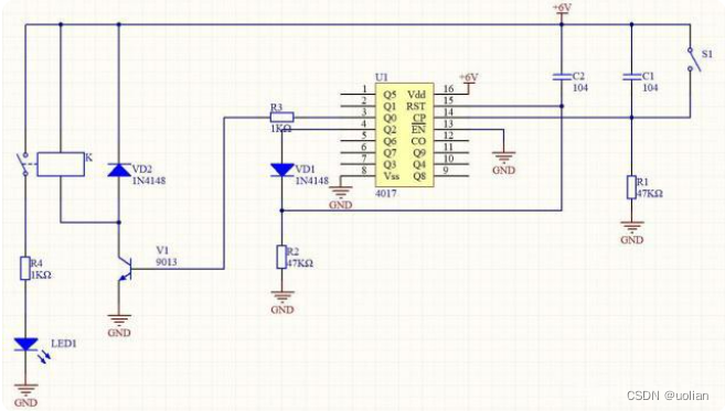
Key control switch
Principle introduction
After the power is turned on, C1 is charged through R1, and it is fully charged in a very short time.R2 and C2 form a power-on reset circuit. When the power is first turned on, C2 can be regarded as a short circuit, so the RST reset terminal of pin 15 of U1 is at a high level, and U1 is reset. In a short time, C2 is charged.Pin 15 returns to low level. At this time, Q0 outputs a high level, which is added to the base of V1 through R3, V1 is turned on, relay K is pulled in, and LED1 is lit, indicating that the controlled circuit is connected.The Q1~Q9 output terminals of U1 are all low level.
When the switch S1 is pressed, C1 is rapidly discharged, the 14th pin of U1 gets the rising edge of the pulse, triggers U1 to start counting, and the output of Q0 changes from high level to low level.Q1 outputs a high level, and Q2 maintains a low level. At this time, V1 is turned off, the relay K is released, and LED1 is turned off, indicating that the controlled circuit stops supplying power.After switch S1 is released, C1 is fully charged again.
When the switch S1 is pressed again, C1 will discharge again, and the 14th pin of U1 will get the counting pulse again, triggering U1 to count again.The high level is added to the RST reset terminal of pin 15 of U1 through VD1 to reset U1, so the output of Q0 becomes a high level, Q1 and Q2 output a low level, V1 is turned on again, the relay K is pulled in, LED1Lights up, indicating that the controlled circuit is energized again and starts to work.Therefore, every time S1 is pressed, the output state of Q0 is reversed once, and the controlled circuit is turned on or off once.
Experimental tips
During the working process of the circuit, when S1 is pressed, C1 will be discharged. When S1 is released, after a short period of time, C1 will be fully charged again, and the 14th pin of U1 will be low level.During this time, any mechanical jitter on switch S1 will also not generate a second technical pulse, thus acting as an anti-jitter.Other outputs of 4017 are not used and can be left floating.
边栏推荐
猜你喜欢
Haproxy搭建web群集
ReentrantLock 原理
SCA兼容性分析工具(ORACLE/MySQL/DB2--->MogDB/openGauss/PostgreSQL)
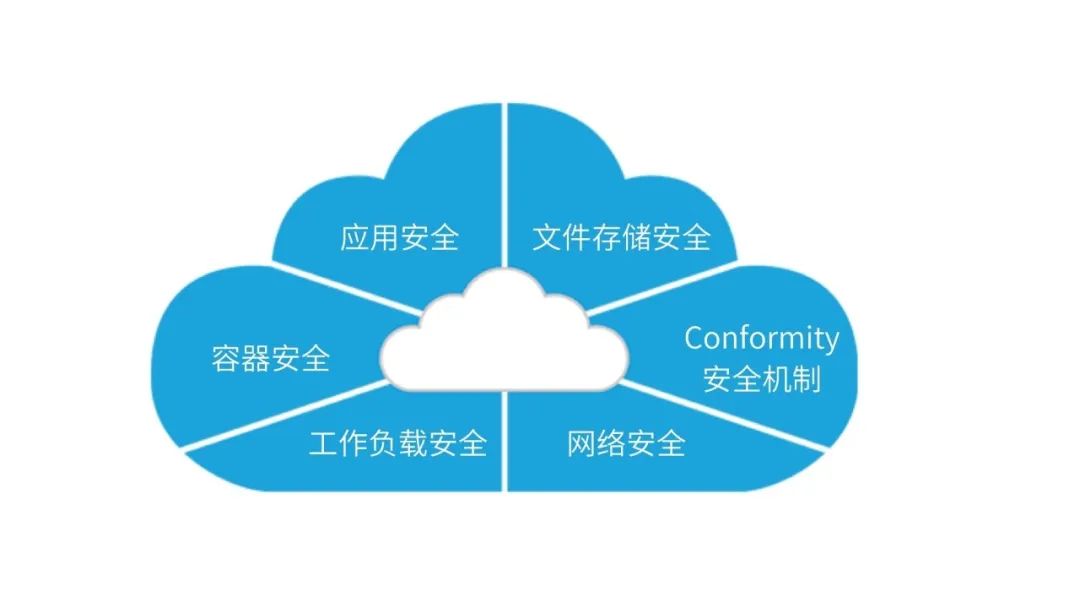
企业应当实施的5个云安全管理策略
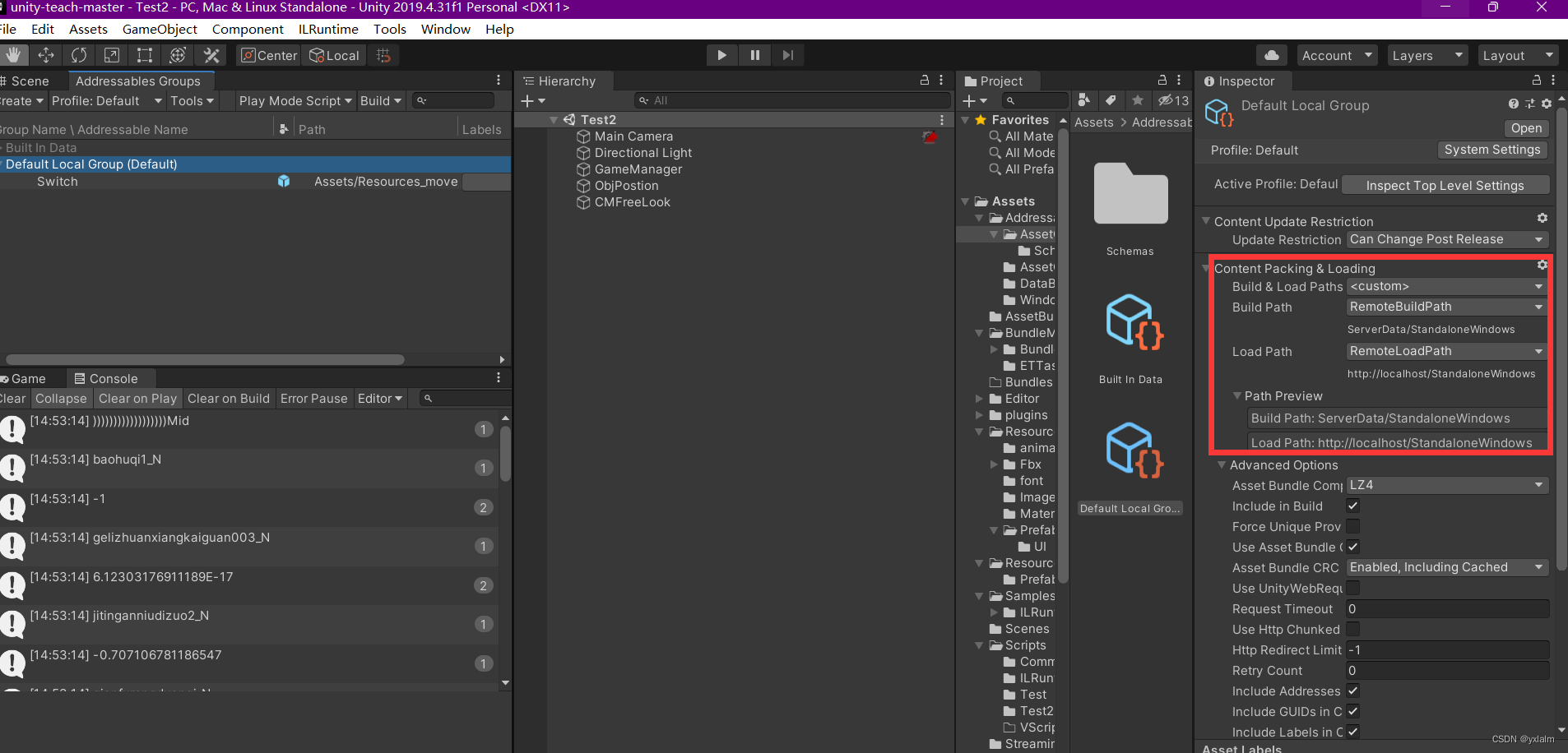
Unity 3D模型展示框架篇之资源打包、加载、热更(Addressable Asset System | 简称AA)
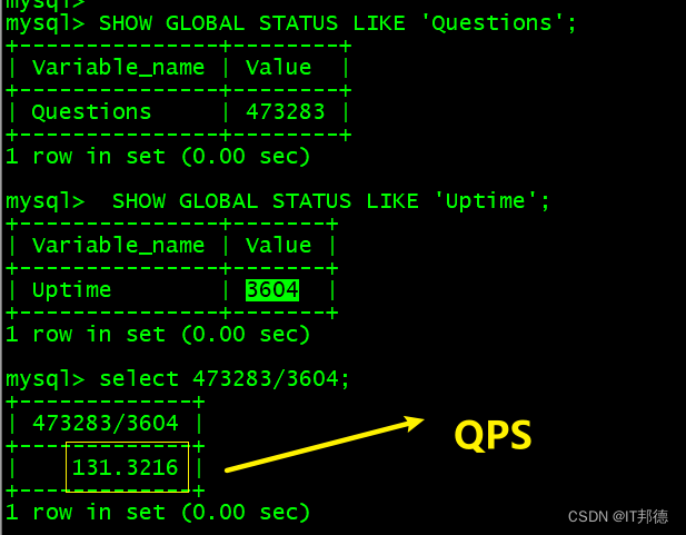
How to stress the MySQL performance indicators TPS\QPS\IOPS?

做项目管理有且有必要了解并学习的重要知识--PMP项目管理
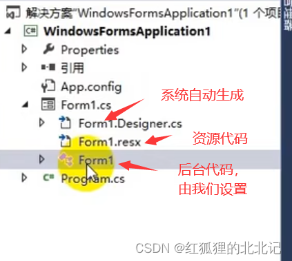
c#之winform(软件开发)

《社会企业开展应聘文职人员培训规范》团体标准在新华书店上架
持续交付(三)Jenkinsfile语法使用介绍
随机推荐
双目立体视觉笔记(二)
【解决方案 三十一】Navicat数据库结构同步
【LeetCode】38、外观数列
nVisual secondary development - Chapter 2 nVisual API operation guide Swagger use
座舱人机交互「暗潮汹涌」,语音「下」,多模态「上」
odoo13 note point
Utility function---string processing
21天学习挑战赛--第二天打卡(setSystemUiVisibility、导航栏、状态栏)
Ceres库运行,模板内报内存冲突问题。(已解决)
npm install出现的各种问题
AutoCAD DWG,DXF文件导出高清图片、PDF
idea永久激活教程(新版)
关于mysql join 的一些说明
JSX use
文字编码 - XML 教程
(记录)异步并发,多线程处理表的统计
Escape character is ‘^]’什么意思?怎么使用telnet
让Web页面中的编辑器支持黏贴或直接拖拽来添加图片「建议收藏」
Interviewer: How to view files containing abc string in /etc directory?
php中的ceil和floo以及round函数「建议收藏」