当前位置:网站首页>Detailed explanation of DDR4 hardware schematic design
Detailed explanation of DDR4 hardware schematic design
2022-07-05 11:02:00 【ltqshs】
As a hardware engineer , We usually receive requests for : The memory configuration of this product is DDR4, Capacity 16Gb(2GB=16Gb).
And we usually need to put this “ Humble ” The needs of , Into specific circuits , How to achieve it ?
Actually , It's simple .DDR4 The hardware design process of can be summarized as : Match one for a platform DDR Memory particles , And ensure that the platform and DDR Memory particles can work normally .
So it can be divided into 2 part , How to select the platform 1 star DDR Memory particles ? How to ensure DDR Relevant circuits can work normally ?
DDR Memory particle selection
At present, many chips will put CPU And peripheral control circuit ( for example :FLASH Control circuit ,DDR Control circuit ,USB Control circuit ) Integrated into the 1 Of the chips , Like Qualcomm MDM8909, Chips like this , We call it “ Platform chip ”. Platform chip DDR Control circuit , We call it “DDR Controller”, Translate it into :DDR controller .
by DDR The controller is matched with what it can control DDR Memory particles , You must first understand :DDR What memory particles does the controller need ?
The first step of hardware design : Refer to the platform chip specification , About DDR Description of the controller section .
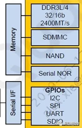
It has d one PCIe gen3, dual USB3.0, multiple serial IOs selectable between
SPI/I2C/UART, Dual SDIO for eMMC and SD card, I2S/PCM/Display Interfaces,16/32 bits DDR3L/4 up to 2400 MT/s, parallel NAND, serial NOR, and Wi-Fi/IOT coexistence interfaces for up to two radios.
So we learned :
The platform chip , Support DDR3L perhaps DDR4 Memory particles , The data bit width is 16 Bits or 32 position , The maximum data transmission speed is 2400MT/s, That is, the frequency is 1200MHz(DDR It is bilateral data transmission ,1 Clock cycles to transmit 2 Time data ,1s Transmitted 2400M Time , That means 1s The clock has changed 1200 Time , That is, the frequency is 1200MHz).
Combined with product requirements : Capacity 16Gb, Then we can basically lock DDR The detailed specifications of .
Before formal model selection , And introduce 1 A concept “RANK”. We know ,DDR That is, it supports multiple memory particles to expand capacity , It also supports multiple memory particles to expand the data bit width .
for example , our DDR Controller support 32 Bit data bit width , Then we can use 8 individual 4 position DDR, perhaps 4 individual 8 position DDR, perhaps 2 individual 16 position DDR, perhaps 1 individual 32 position DDR Data bit expansion . If we use 8 individual 4 position DDR Particles are designed , our RANK The quantity is 8, We call it “8-RANK Design ”, In practice, of course , We are definitely not so stupid , take 8 individual 4 position DDR To expand 32 position .
therefore , Then confirm our RANK After the quantity , Demand is locked . The capacity is set to 16Gb, The type is DDR4, Data width is 32 position , The highest frequency is 1200MHz. Because at present most of DDR Memory particles are supported at most 16 Bit data width , therefore RANK The number of 2, That's what we call Dual-RANK Design .
According to this requirement , Can be in DDR Go to the official website to find the right “DDR chip ” 了 . For example, on the product page of MgO official website , selected DRR4-SDRAM, selected 8Gb,DDR4.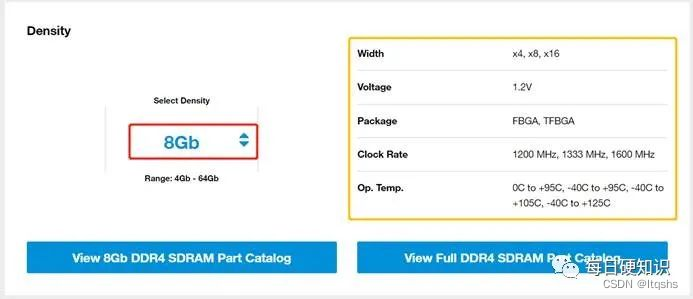
The website will recommend many models for you . For example, the data bit width is 8 Bit , You can skip .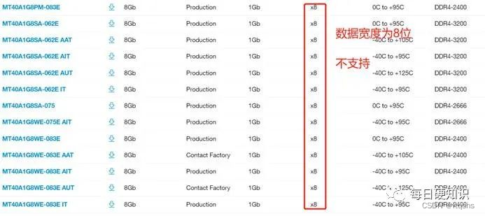
The data bit width is 16 position , The frequency is 1200Mhz(2400MT/s) Of , There is still a lot of . This is the time to test the professional quality of hardware engineers , We should not only consider hardware performance , Also consider the cost of materials , Material purchase cycle . Consideration cost , Try not to have “ Designed ” The place of , So the rate is 3200MT/s The device is excluded . If we are consumer commercial products , Therefore, choose a narrow temperature range of commercial devices , secondly , In order to enhance your relationship with purchasing ,
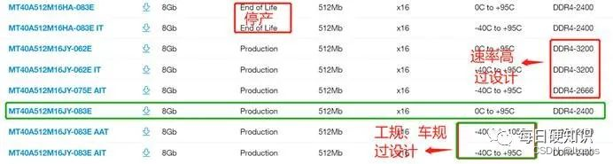
So down , Our selection is basically focused on MT40A512M16JY-083E 了 , The dosage is 2 slice .
here , Start reading device specifications , Understand electrical performance , Design peripheral circuit , Give Way DDR Controller and DDR Memory particles are running happily .
DDR Hardware circuit construction
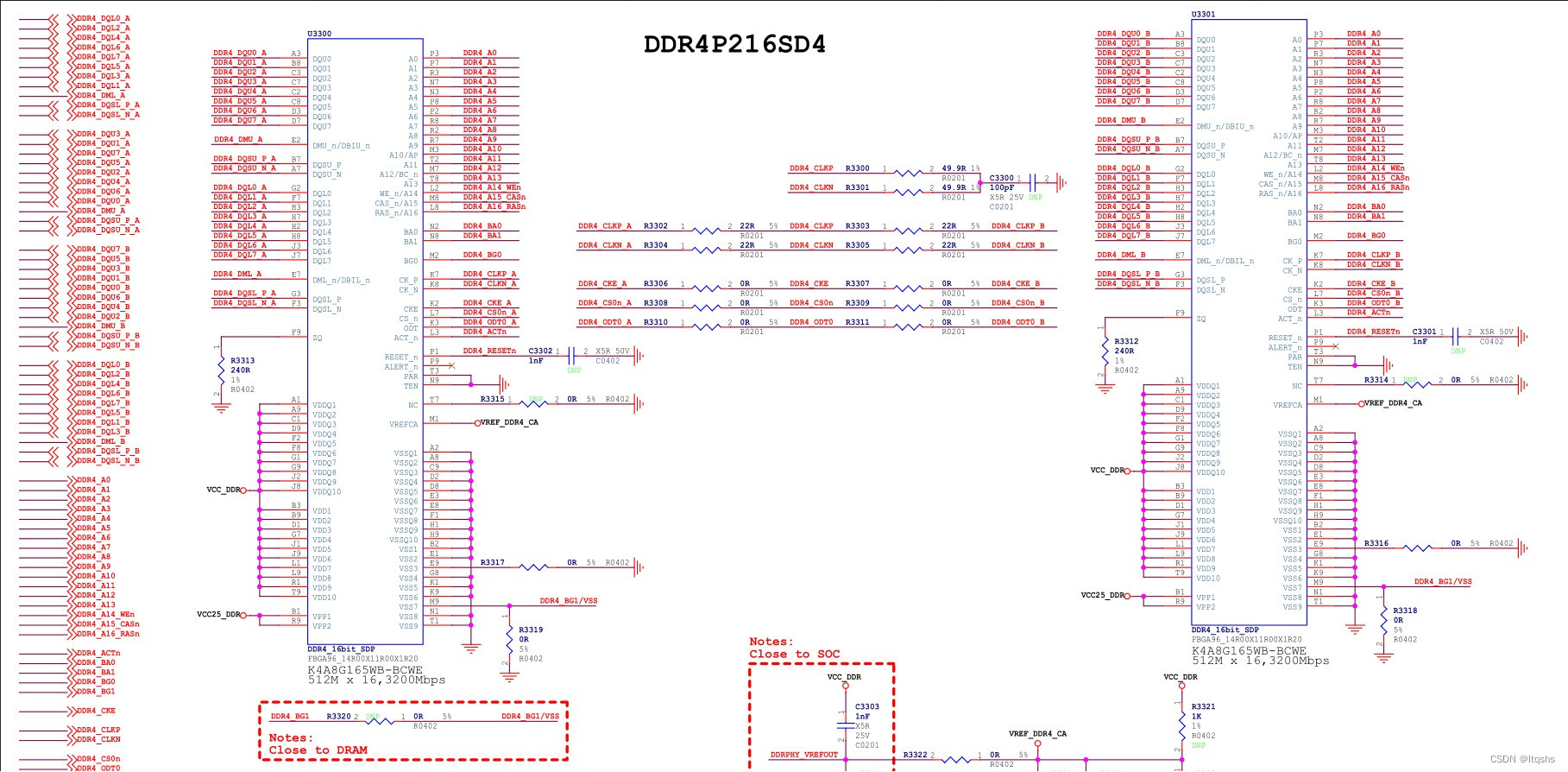
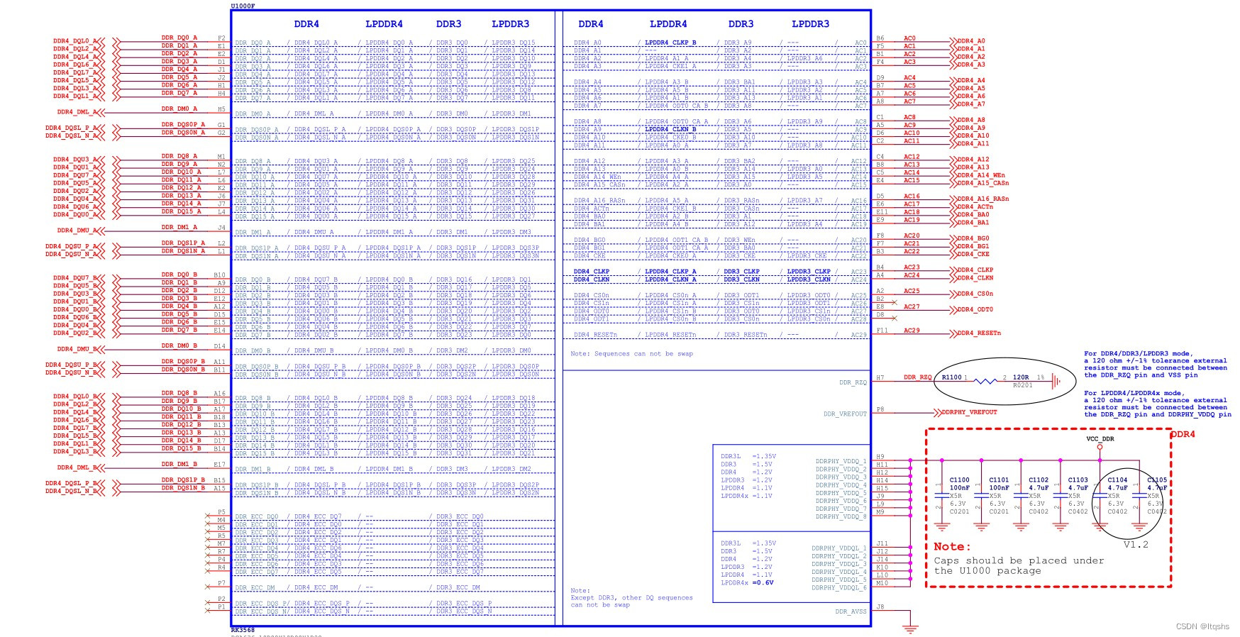
Design logic device circuit , We must have logical thinking , The simplest logical thinking , Grouping is . therefore , First understand DDR Hardware interface of controller . Controller hardware PIN The feet can be divided into power packs , Configuration group , Control group , Clock group , Address group , Data sets .
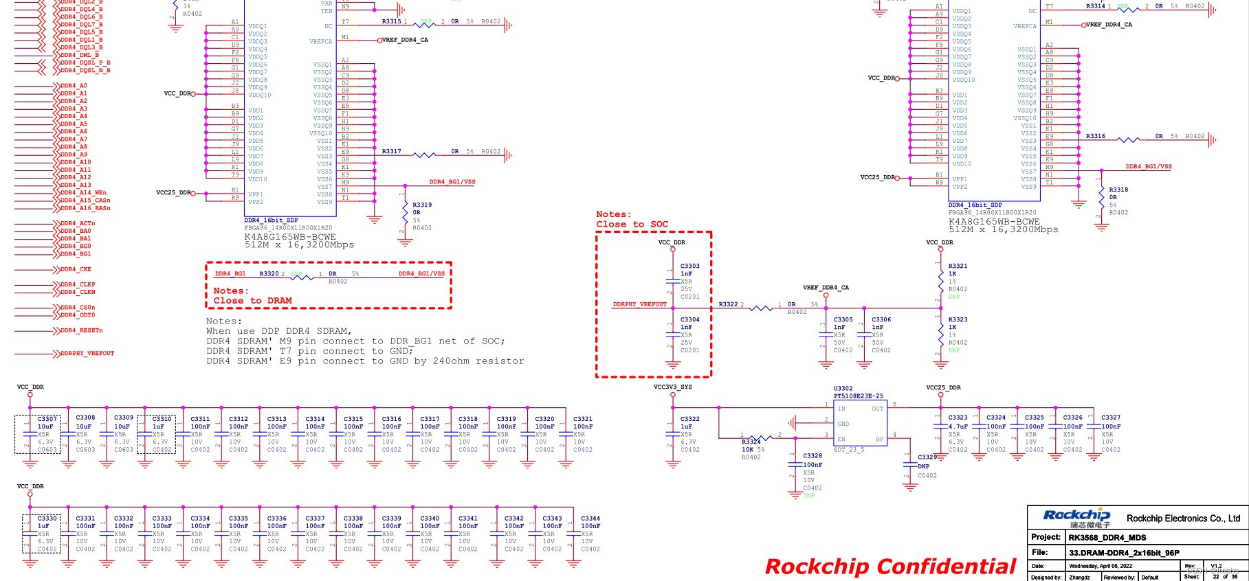
The interfaces of power pack and configuration group are as follows , Power supply , Connect the resistance to complete ,1.2V Power supply of , Be as smooth as possible , Here to ignore .ZQ Resistance is used to calibrate ODT Impedance , We'll talk about that later .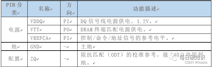
The control group interface is as follows .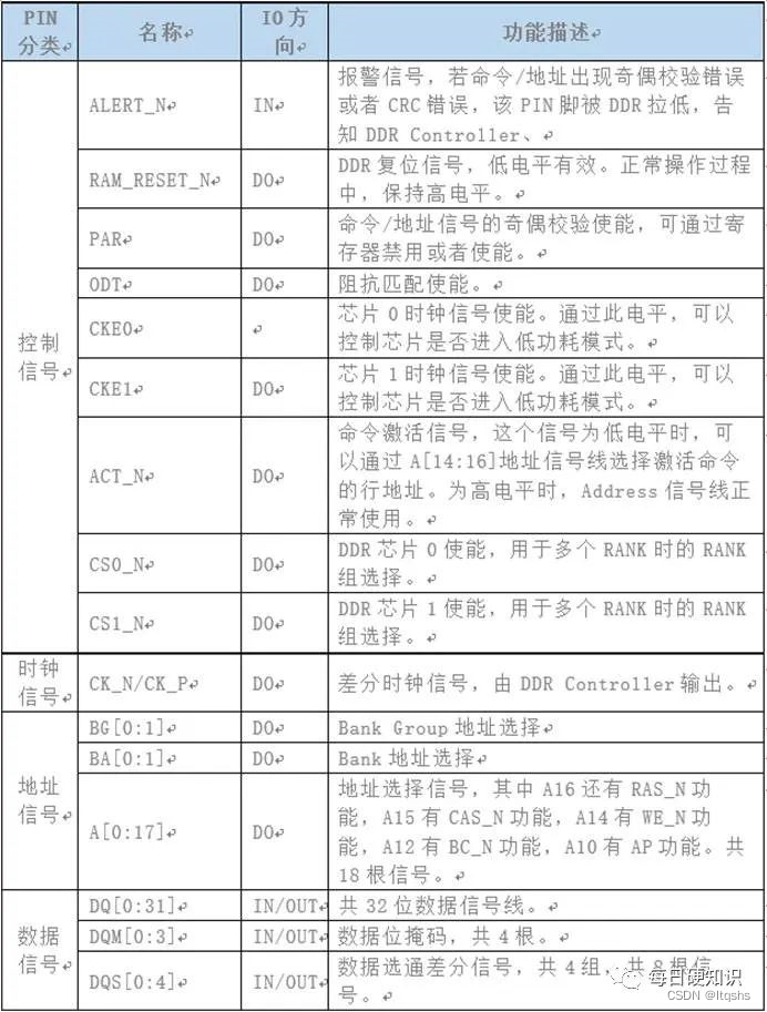
After grouping , According to DDR To design the peripheral hardware .
In the control signal , We need to pay attention to CS0 and CS1,2 A chip selection signal can be used for , many RANK Memory capacity expansion , explain DDR controller , Most support 2 Group RANK. Each group RANK Assign a separate chip selection signal . We design here 2 individual 16 Bit chip composition 1 individual RANK, namely CS0 At the same time, connect to the currently selected 2 individual DDR Granular CS On , Form a daisy chain . Other control signals generally have no timing requirements , It is enough to pass logic .
The address signal usually refers to the clock signal , To address , Therefore, the address signal should be strictly consistent with the length of the clock signal , To ensure that all address bits arrive at the same time when sampling . Because on the same board , The transmission speed of electrons on each wire is the same , So the length of the signal line is about , The later the signal arrives , The shorter the length of the signal line , The sooner the signal arrives , When address sampling , There is a time limit , therefore , All address signals must be within the sampling time range , All arrive at , Therefore, it is required to control the length of the address line relative to the clock line . In the previous section, we talked about the principle of memory addressing , First use BG Signal selection BANK GROUP, Reuse BA The signal goes on BANK choice , Reuse A[0:16] Select rows and columns , Reuse A[0:16] Make column selection , Complete addressing . You can see ,Address The signal is used for row selection and column selection ,BG and BA Signals are kept , therefore BG Signals and BA The equal length requirement of the signal will be relatively wide .
DDR The controller has 2 root BG The signal ,2 root BA The signal ,17 root Address The signal , The same RANK Yes 2 individual DDR Grain , Every DDR Particles have 1 root BG The signal ,2 root BA The signal ,17 root Address The signal , front CS0 At the same time 2 individual DDR Film selection of particles , So when addressing two DDR Will be selected at the same time , that DDR How the controller distinguishes between addressing 1 star DDR Particles ? How to connect the hardware ? It's very simple , According to the memory addressing principle mentioned in the previous section , We know everything DDR Particles have 2 individual BANK GROUP(1 root BG The signal ),4 individual BANK(2 root BA The signal ), And CS The principle of capacity expansion is consistent , We put BG0 Connect to DDR Grain 1 On ,BG0 Pull up and pull down , We can address CHIP1 Of 8 individual BANK.BG1 Connect to DDR Grain 2 On ,BG1 Pull up and pull down , We can address CHIP1 Of 8 individual BANK.BA、ADDR Daisy chain connection , Connect at the same time 2 star DDR On chip .
Next , Let's look at the links of data signals , Data signals are internally grouped , because DDR When data signals are transmitted, both sides are transmitted along the data , And if all signals are equal in length with reference to the clock , It will make equal length control very difficult , increase DDR The difficulty of design , So smart humans came up with another trick , An additional data strobe signal is added as the sampling clock of the data signal , Every time 8 Bit signal , Refer to a set of differences . So we can easily see DDR The controller has 4 Group DQS Differential signal ,32 Root data signal . our RANK There is 2 individual DDR Grain , Each particle has 2 Group DQS Differential signal ,16 Root data signal . therefore
Controller DQS[0:1] Connect DDR CHIP0 Of DQS[0:1],
Controller DQ[0:15] Connect DDR CHIP0 Of DQ[0:15].
Controller DQS[2:3] Connect DDR CHIP1 Of DQS[0:1],
Controller DQ[16:31] Connect DDR CHIP1 Of DQ[0:15].
Reference article :《DDR4 Detailed hardware design 》
边栏推荐
- BOM//
- 运算符、、
- 如何让全彩LED显示屏更加节能环保
- 2022年化工自动化控制仪表考试试题及在线模拟考试
- Network security of secondary vocational group 2021 Jiangsu provincial competition 5 sets of topics environment + analysis of all necessary private messages I
- 2022年流动式起重机司机考试题库及模拟考试
- Wechat nucleic acid detection appointment applet system graduation design completion (8) graduation design thesis template
- 磨砺·聚变|知道创宇移动端官网焕新上线,开启数字安全之旅!
- 【tcp】服务器上tcp连接状态json形式输出
- 脚手架开发进阶
猜你喜欢
A mining of edu certificate station
matlab cov函数详解
2022鹏城杯web
九、磁盘管理
Talk about the understanding of fault tolerance mechanism and state consistency in Flink framework
Do you really understand the things about "prototype"? [part I]

2022年流动式起重机司机考试题库及模拟考试
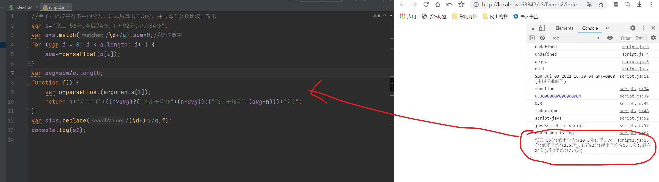
【JS】提取字符串中的分数,汇总后算出平均分,并与每个分数比较,输出

The first product of Sepp power battery was officially launched
关于 “原型” 的那些事你真的理解了吗?【上篇】
随机推荐
vite//
Bracket matching problem (STL)
GBase 8c数据库如何查看登录用户的登录信息,如上一次登录认证通过的日期、时间和IP等信息?
[TCP] TCP connection status JSON output on the server
LDAP overview
【DNS】“Can‘t resolve host“ as non-root user, but works fine as root
2022年流动式起重机司机考试题库及模拟考试
Applet framework taro
Web Components
流程控制、
2022年化工自动化控制仪表考试试题及在线模拟考试
How can gbase 8C database view the login information of the login user, such as the date, time and IP of the last login authentication?
2021 Shandong provincial competition question bank topic capture
DDRx寻址原理
Nuxt//
关于vray 5.2的使用(自研笔记)
基于昇腾AI丨爱笔智能推出银行网点数字化解决方案,实现从总部到网点的信息数字化全覆盖
Question bank and answers of special operation certificate examination for main principals of hazardous chemical business units in 2022
括号匹配问题(STL)
Web3基金会「Grant计划」赋能开发者,盘点四大成功项目