当前位置:网站首页>OC and OD gate circuit
OC and OD gate circuit
2022-07-05 08:09:00 【Learning notes of hardware Xiaobai】
Students who have studied digital and analog electricity , I should have heard of it all OC Gate circuit and OD Gate circuit . Even if you haven't heard of it , Then when I graduated and went for a job interview , May be asked by the interviewer or in the exam . Because many chips IO mouth , Its interior belongs to OC perhaps OD door . Think of last year , When the editor is interviewing for a job , The interviewer has asked this question , It was called a “ Miserable ” ah !
As a hardware engineer , Although in circuit design , This kind of circuit is rarely encountered , But its circuit form and working principle must be understood .
So Xiaobian still needs to talk about OC Door and OD door .
OC door 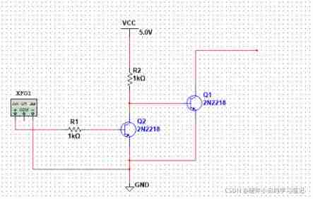
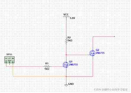
OC The collector of the gate is open . That is, the collector of the triode is not connected . When the left end input is low , The output of the triode at the right end is low . However, when the left end input high level , Because the collector of the triode at the right end is in an open circuit state , Therefore, high level cannot be output . Therefore, if you want to output a high level on the right side, you need to pull up the resistance and external power supply to meet the high level output .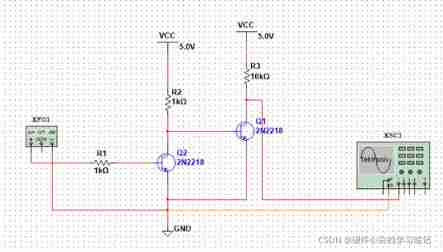
here :
- The input is high power level ,Q1 Conduction , here A Point is in low level , Unable to meet Q2 Conduction , Now Q2 To break off , The output is high level .
- The input is low power level ,Q1 To break off , here A Point is in high level ,Q2 Conductive , At this time, the output voltage is low .
OC The door uses a pull-up resistor to output a high level . Selection of resistance , We should choose from the principle of driving current and reducing power consumption .
The figure shows the simulated waveform 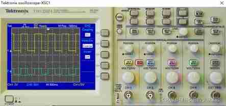
We will find that there is a downward pulse , At this time, a suitable capacitor can be added to solve this kind of problem .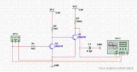
Simulation oscillogram 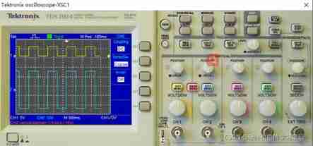
OD door
The understanding idea is the same as that of open collector .
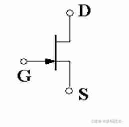
OD The gate is open drain . That is, the rightmost MOS The drain of the tube is not connected to anything . When the left end input is low , Right end MOS The tube output is low . However, when the left end input high level , Due to the MOS The tube drain is open , Therefore, high level cannot be output . Therefore, if you want to output a high level on the right side, you need to pull up the resistance and external power supply to meet the high level output .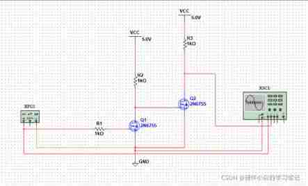
This figure is the waveform of simulation , There will be a small number of pulses , The voltage is about 0.5V Rise .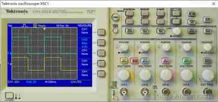
To avoid this problem , Try adding a suitable capacitor at the output , To remove this interference . The addition of capacitance will also appropriately reduce the rising speed of level conversion . At the same time, the choice of pull-up resistance is also a factor that determines the rising speed . according to RC The delay circuit knows , resistance , The greater the capacitance , The lower the rising speed , However, resistance has the advantage of reducing power consumption . Therefore, the selection of the pull-up resistance value , Still need to balance power consumption and rising speed .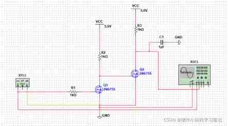
Capacitive effect :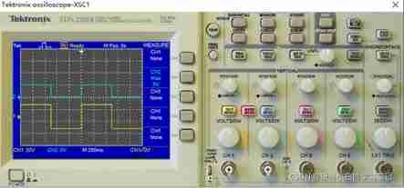
边栏推荐
- IEEE access personal contribution experience record
- Zero length array in GNU C
- Create inf module in AMI code
- Random function usage notes
- Management and use of DokuWiki (supplementary)
- Problem solving: interpreter error: no file or directory
- How to migrate the device data accessed by the RTSP of the easycvr platform to easynvr?
- solver. Learning notes of prototxt file parameters
- Classic application of MOS transistor circuit design (2) - switch circuit design
- 研究发现,跨境电商客服系统都有这五点功能!
猜你喜欢
Basic embedded concepts
Create inf module in AMI code
Semiconductor devices (III) FET
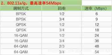
Wifi-802.11 negotiation rate table
![C WinForm [help interface - send email] - practice five](/img/2a/c4e7abe054e6fdd45acc7d297a033d.jpg)
C WinForm [help interface - send email] - practice five
Cadence simulation encountered "input.scs": can not open input file change path problem
![Halcon's practice based on shape template matching [1]](/img/68/206eed7502fbf108a929aa9365b1ae.jpg)
Halcon's practice based on shape template matching [1]

Matlab2018b problem solving when installing embedded coder support package for stmicroelectronic
![C WinForm [display real-time time in the status bar] - practical exercise 1](/img/9f/d193cbb488542cc4c439efd79c4963.jpg)
C WinForm [display real-time time in the status bar] - practical exercise 1

C language # and #
随机推荐
Pointnet++ classification practice
Live555 push RTSP audio and video stream summary (III) flower screen problem caused by pushing H264 real-time stream
Why is 1900 not a leap year
C WinForm [help interface - send email] - practice five
Communication standard -- communication protocol
C, Numerical Recipes in C, solution of linear algebraic equations, LU decomposition source program
My-basic application 2: my-basic installation and operation
C WinForm [view status bar -- statusstrip] - Practice 2
Cadence simulation encountered "input.scs": can not open input file change path problem
Record the visual shock of the Winter Olympics and the introduction of the screen 2
How to migrate the device data accessed by the RTSP of the easycvr platform to easynvr?
[trio basic tutorial 18 from introduction to proficiency] trio motion controller UDP fast exchange data communication
Adaptive filter
Fundamentals of C language
Semiconductor devices (I) PN junction
H264 (I) i/p/b frame gop/idr/ and other parameters
导电滑环磨损快的原因
Problem solving: interpreter error: no file or directory
Gradle复合构建
找不到实时聊天软件?给你推荐电商企业都在用的!