当前位置:网站首页>Classic application of MOS transistor circuit design (1) -iic bidirectional level shift
Classic application of MOS transistor circuit design (1) -iic bidirectional level shift
2022-07-05 08:06:00 【Learning notes of hardware Xiaobai】
MOS tube , As one of the most important components in hardware design , It will be used in many application scenarios .
In circuit design , Level conversion circuit is an indispensable part . In terms of power supply , In addition to system power supply , In many other cases, level conversion circuits are needed , To get the voltage we need . At the same time, there are various circuits in level conversion , One of them is useful to MOS Case of management . So today, , Xiaobian will explain to you MOS Application of transistor in level conversion circuit .
two-way level shift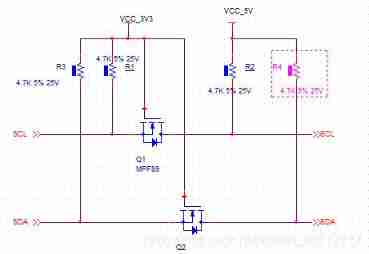
This circuit belongs to IIC Level conversion circuit . The main use is NMOS tube . Connected in series with clock and data signal lines respectively . For convenience , Let me introduce SCL Level conversion on this line .
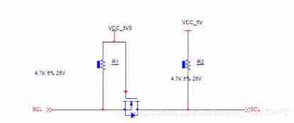
As a clock line , Nothing more than low level , Or high level .
So , This line is divided into four situations .
When the left end is pulled low, it is the low level ,Vgs=3.3V.
here MOS The pipe is open , The signal on the right is also in a low-level state .When the left end is pulled high, it is the high level .Vgs=0V.
here MOS Pipe cut off ,MOS The pipe is not connected . The left end is still high , be in 5V.
On the line , The left end is 3.3V, On the right is 5V. That is to form 3.3V turn 5V Level transition state of .
When the right end is pulled low, it is the low level
here MOS The diode of the tube is on , At this time, the left end is also in a low-level state .When the right end is pulled high, it is the high level .
here MOS Pipe cut off , The left end is high 3.3V.
On the line , The left end is 3.3V, On the right is 5V., That is to form 5V turn 3.3V Level transition state of .
Circuit design considerations
- MOS Tube selection enhanced depletion NMOS tube .
- NMOS tube , The left and right ends are adjustable , but S The pole voltage is always less than G Pole voltage .
- MOS Tube on voltage Vgs(th) Slightly less than level shift Left end level value .
- IIC Different selection rates , Yes MOS The switching time of the tube is required . The data has a time difference from left to right . On the one hand, this time is affected by MOS The closing time parameter of the tube affects , On the other hand, it is affected by the capacitive reactance of the bus + Effect of pull-up resistance (RC Time constant ). The most common is I2C The transmission rate is 400kbit/s. namely 1bit The transmission time of is 2.5us,MOS Tube when selecting , Its switching time should also be less than this value . Otherwise , Here 2.5us within ,1 The transmission of bit data may not meet the requirements of timing , Cause communication failure .
In addition ,MOS Tube is doing 3.3V turn 5V On the level conversion circuit , And here's more , It is also one of the most common methods .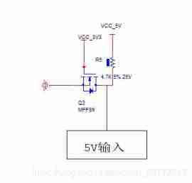
边栏推荐
- Record the opening ceremony of Beijing Winter Olympics with display equipment
- Altium designer 19.1.18 - change the transparency of copper laying
- Interview catalogue
- [trio basic tutorial 17 from getting started to mastering] set up and connect the trio motion controller and input the activation code
- Factors affecting the quality of slip rings in production
- How to excavate and research ideas from the paper
- Define in and define out
- C language # and #
- C WinForm [realize the previous and next selection pictures] - practice 7
- 导电滑环磨损快的原因
猜你喜欢
UEFI development learning 2 - running ovmf in QEMU
![C WinForm [change the position of the form after running] - Practical Exercise 4](/img/f7/ddaf5773295ca6929d39d7aa760d36.jpg)
C WinForm [change the position of the form after running] - Practical Exercise 4
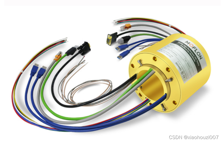
Factors affecting the quality of slip rings in production
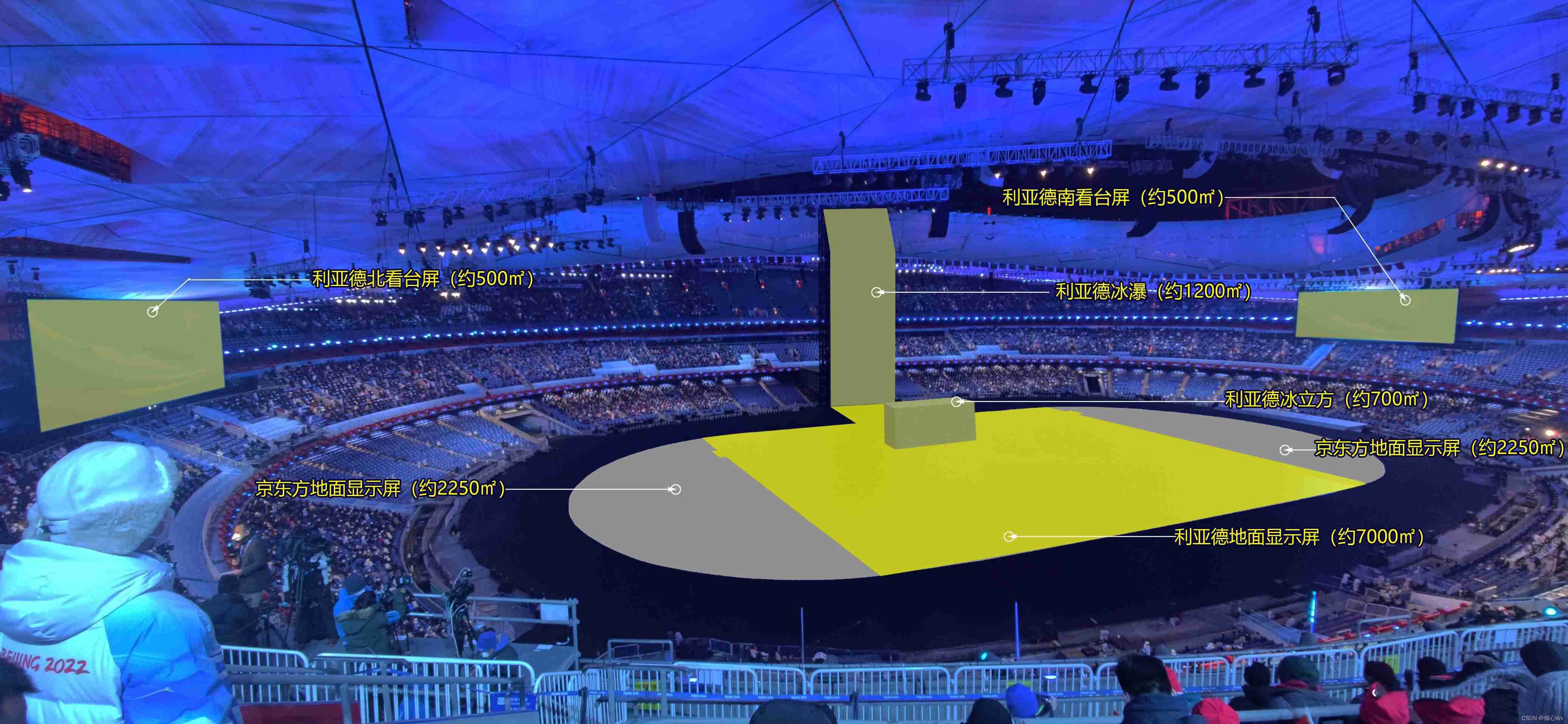
Record the visual shock of the Winter Olympics and the introduction of the screen 2

C # joint configuration with Halcon

找不到实时聊天软件?给你推荐电商企业都在用的!

UEFI development learning 5 - simple use of protocol
![[trio basic tutorial 16 from introduction to proficiency] UDP communication test supplement](/img/54/78e4e10724b2762274b06debb10877.jpg)
[trio basic tutorial 16 from introduction to proficiency] UDP communication test supplement
Process communication mode between different hosts -- socket

Programming knowledge -- assembly knowledge
随机推荐
C language enhancement -- pointer
MLPerf Training v2.0 榜单发布,在同等GPU配置下百度飞桨性能世界第一
Global and Chinese markets for recycled boilers 2022-2028: Research Report on technology, participants, trends, market size and share
C#,数值计算(Numerical Recipes in C#),线性代数方程的求解,LU分解(LU Decomposition)源程序
Create inf module in AMI code
matlab timeserise
UEFI development learning 2 - running ovmf in QEMU
L'étude a révélé que le système de service à la clientèle du commerce électronique transfrontalier a ces cinq fonctions!
Some tips for using source insight (solve the problem of selecting all)
Beijing Winter Olympics opening ceremony display equipment record 3
My-basic application 2: my-basic installation and operation
导电滑环磨损快的原因
Consul安装
Class of color image processing based on Halcon learning_ ndim_ norm. hdev
UEFI development learning 5 - simple use of protocol
Relationship between line voltage and phase voltage, line current and phase current
Fundamentals of C language
C WinForm [view status bar -- statusstrip] - Practice 2
LED display equipment records of the opening ceremony of the Beijing Winter Olympics
Explication de la procédure stockée pour SQL Server