当前位置:网站首页>08-SDRAM: Summary
08-SDRAM: Summary
2022-08-02 00:16:00 【Liu Yaner】
前言
推荐阅读:孤独的单刀 - SDRAM汇总篇
正文
一、SDRAM概念
1.1 含义
SDRAM(Synchronous Dynamic Random Access Memory),同步动态随机存储器
同步:
动态:Continuous refresh to ensure the reliability of data(电容存储电荷)
随机:
1.2 版本
- SDR SDRAM:即常说的SDRAM,采用
single-ended clock signal,在Sampled on the rising edge of the clock - DDR SDRAM
- DDR2 SDRAM
- DDR3 SDRAM
- DDR4 SDRAM
时钟信号:差分信号(抗干扰)
采样模式:Both rising and falling edges of the clock are sampled
1.3 存储阵列
SDRAM中4area for storage,即4个Bank
SDRAM 存储容量计算:
- Find the corresponding line address in the chip manual、The bit width of the column address,下面图中Bank的行数=13,列数=9
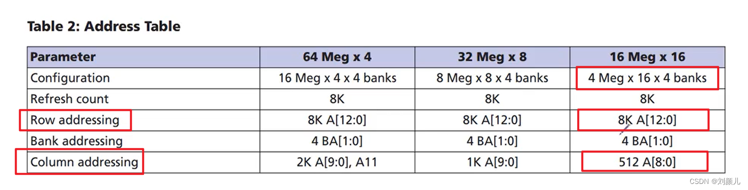
- Assume that each storage unit can store16bit的数据
- 计算公式:
(2^13) * (2^9) * 16 bit * 4 Bank = 256Mbit (单位是bit)
1.4 芯片引脚
CLK:时钟
CKE:时钟使能,高电平时,CLK才起作用
RAS#:低电平有效,行选通信号
CAS#:低电平有效,列选通信号
这2pins are used in commonA0-A12这13个引脚,分时复用
WE#:使能写操作、预充电
CS#:片选信号,Shield or enable all input and output ports
SDRAM操作命令:CS#——CAS#——RAS#——WE#
BA[1:0]:Bank地址
A[12:0]:存储地址
DQ[15:0]:双向数据端口
1.5 操作命令
1.6 学习难点
It is mainly reflected in the strict requirements on the control sequence
1.6.1 Difficulties caused by dynamics
1.6.2 Difficulties caused by randomness
行地址、Column addresses share one port,分时复用
二、实验
2.1 初始化
The timing diagram is from the Micron data sheet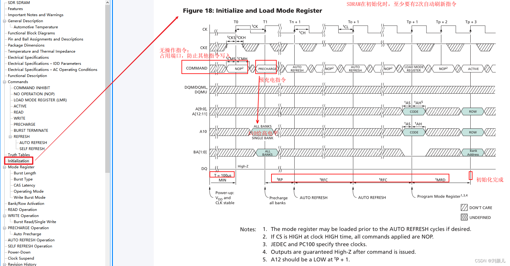
The waveform graph is from Wildfire Video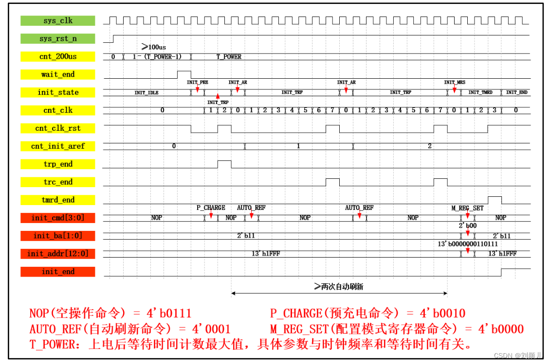
2.1.1指令:
The write of the instruction takes only one clock cycle
SDRAMThe initialization needs to use the following4command together
 parameter   P_CHARGE     =   4'b0010 , //预充电指令 AUTO_REF = 4'b0001     ,   //自动刷新指令
              NOP         =   4'b0111 , //空操作指令 M_REG_SET = 4'b0000     ;   //模式寄存器设置指令

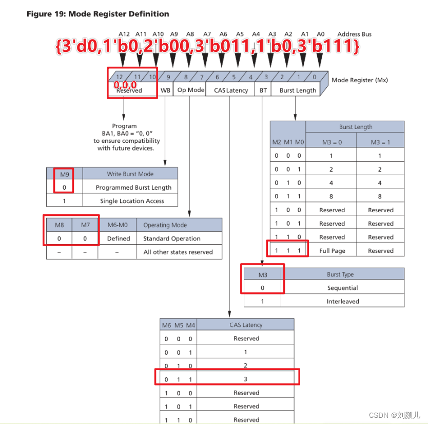
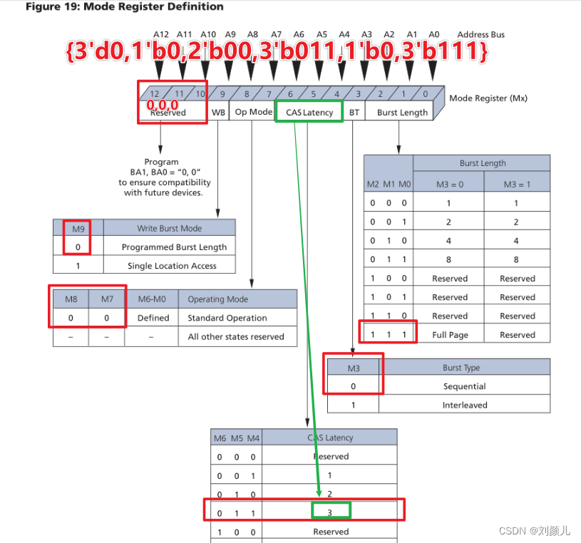
2.1.2 地址
init_addr = {
    3'd0,1'b0,2'b00,3'b011,1'b0,3'b111};
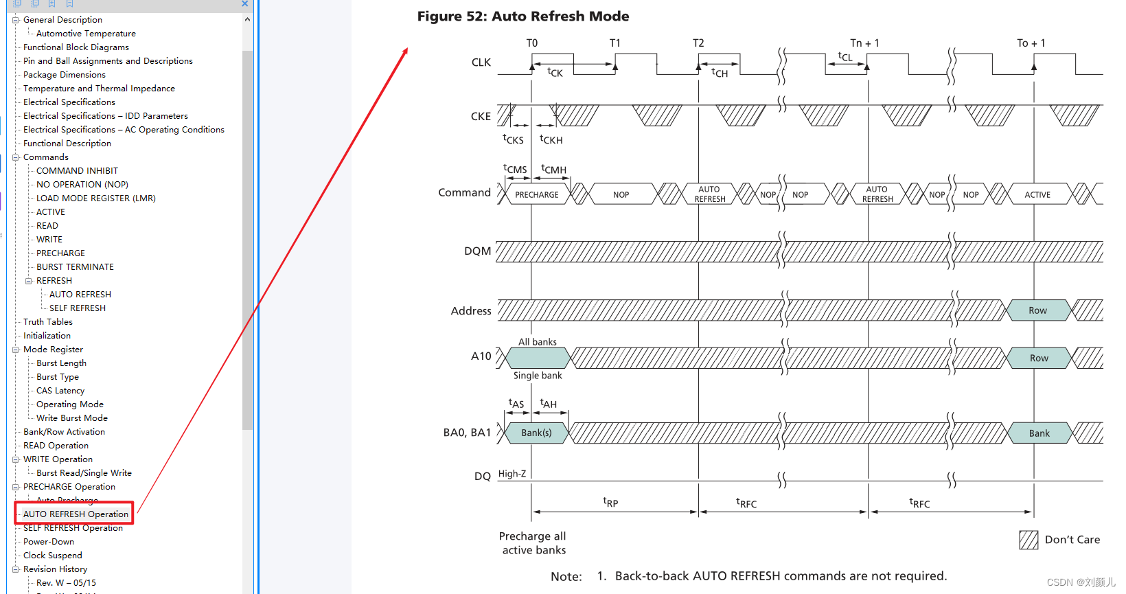
2.2 自动刷新(保证数据不丢失)


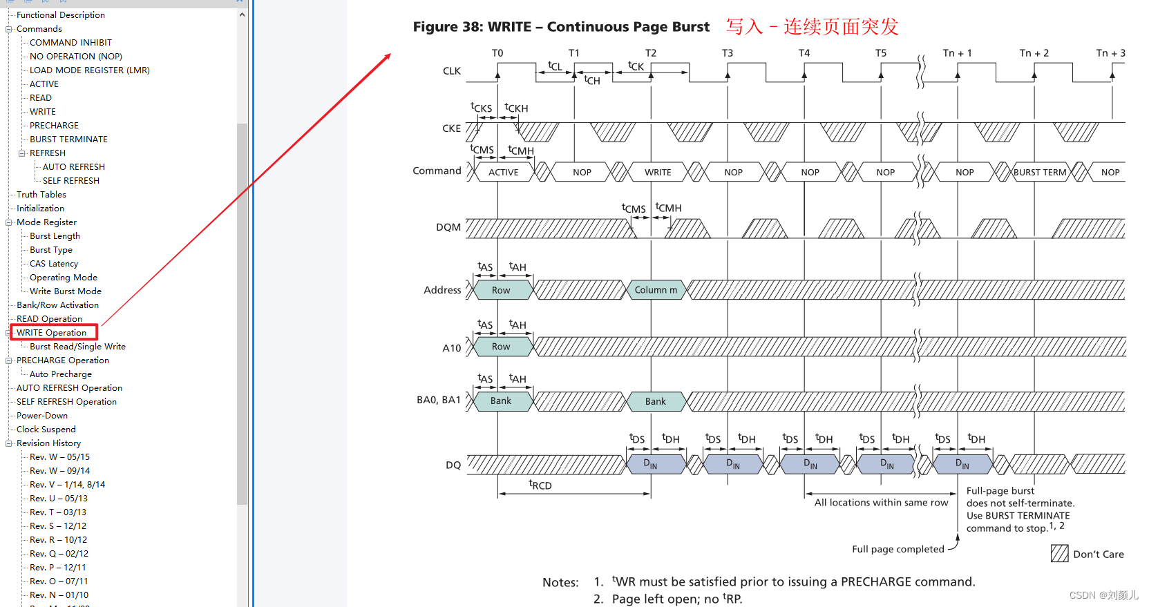
2.3 写操作(页突发)
突发模式:Page burst mode without automatic charging
length of page burst : The number of memory cells contained in a row

2.4 读操作(页突发)
突发模式:Page burst mode without automatic charging
设置潜伏期
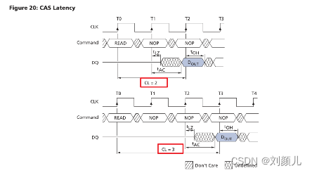
Set in the initialization module section3个潜伏期
So read the data part,就需要用突发长度+3to indicate the cycle of read data usage

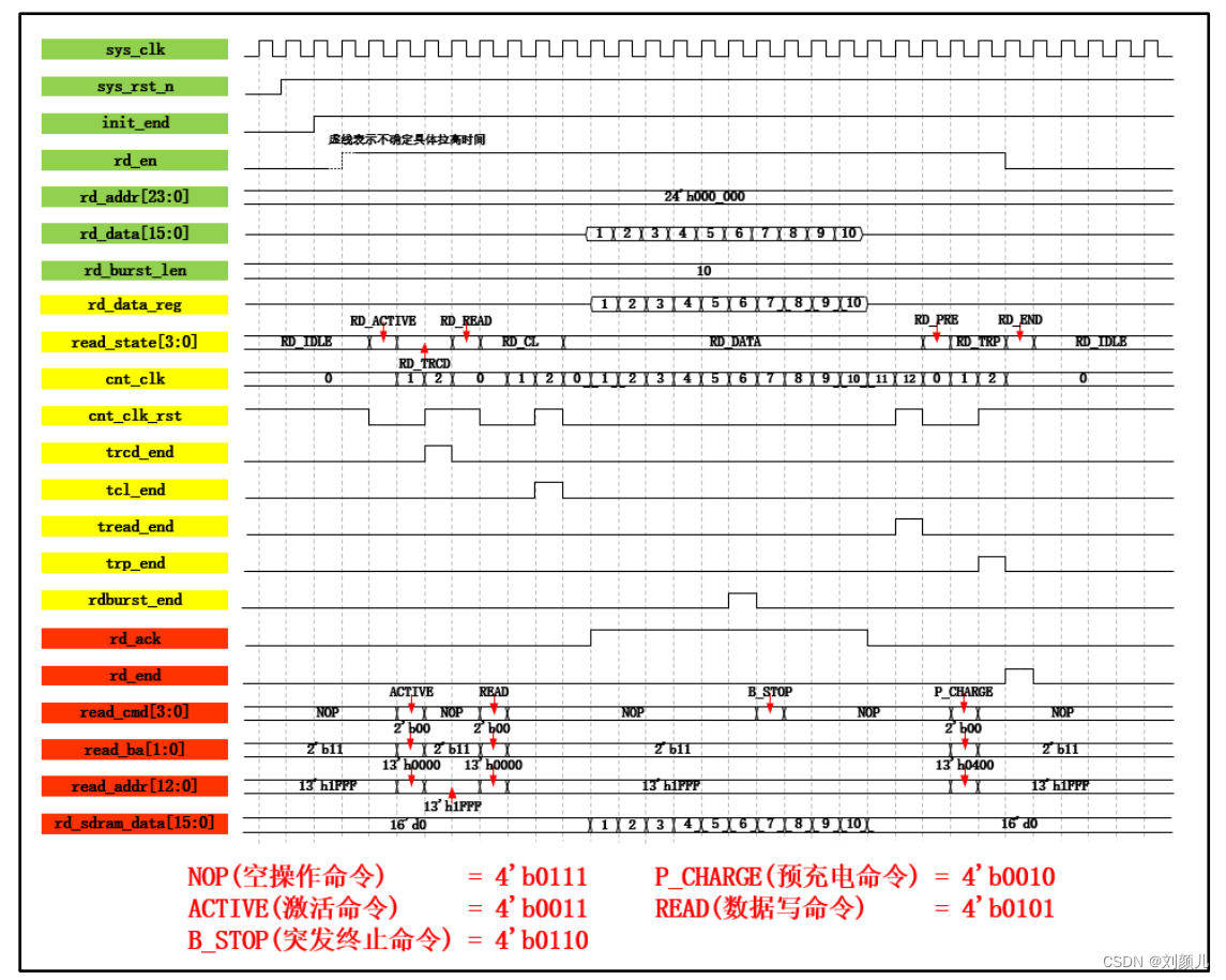
从SDRAMThe data read in need to be tapped,因为SDRAMthe working clock of the current module and the system clock of the current module频率相同、相位不同
2.5 仲裁模块
优先级:自动刷新>写操作>读操作

2.6 SDRAM控制模块
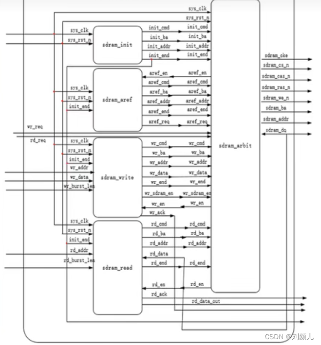
2.7 FIFO控制模块
Need to configure read and writeFIFO的IP核:FIFOIP核配置步骤


边栏推荐
猜你喜欢


![[Headline] Written test questions - minimum stack](/img/67/08f2be8afc780e3848371a1b5e04db.png)


随机推荐
短视频SEO优化教程 自媒体SEO优化技巧方法
双队列实现栈?双栈实现队列?
ES中SQL查询详解
在MySQL中使用MD5加密【入门体验】
JSP如何使用request获取当前访问者的真实IP呢?
控制电机的几种控制电路原理图
Arduino 基础语法
windows sql server 如何卸载干净?
【MySQL系列】 MySQL表的增删改查(进阶)
Axure教程-新手入门基础(小白强烈推荐!!!)
DOM 事件及事件委托
如何优雅的消除系统重复代码
为什么要使用MQ消息中间件?这几个问题必须拿下
QML package management
【Leetcode】475. Heaters
Flink Yarn Per Job - 提交流程一
检查 Oracle 版本的 7 种方法
在不完全恢复、控制文件被创建或还原后,必须使用 RESETLOGS 打开数据库,解释 RESETLOGS.
security CSRF漏洞保护
Is TCP reliable?Why?