当前位置:网站首页>Imx6ul development board porting EMMC startup process of mainline u-boot
Imx6ul development board porting EMMC startup process of mainline u-boot
2022-06-11 12:39:00 【Zhaokaixin xiansen】
Directly in U-Boot The source code downloaded from the official website can be compiled directly in our imx6ul Running on the development board , But what I read DRAM The capacity is wrong , Now analyze the startup process , Confirm what caused the problem . First of all, it must be a well-known board_init_f function
 The function path file is board/engicam/common/spl.c
void board_init_f(ulong dummy)
{

        ccgr_init();

        /* setup AIPS and disable watchdog */
        arch_cpu_init();

        if (!(is_mx6ul()))
                gpr_init();

        /* iomux */
        SETUP_IOMUX_PADS(uart_pads);

        /* setup GP timer */
        timer_init();

        /* UART clocks enabled and gd valid - init serial console */
        preloader_console_init();

        /* DDR initialization */
        spl_dram_init(); // This is the function we need to focus on
}
The expansion is the following function
In the file u-boot/board/engicam/common/spl.c in
static void spl_dram_init(void)
{

        mx6ul_dram_iocfg(mem_ddr.width, &mx6_ddr_ioregs, &mx6_grp_ioregs);
        mx6_dram_cfg(&ddr_sysinfo, &mx6_mmcd_calib, &mem_ddr);
        udelay(100);
}
And then it goes on
u-boot/arch/arm/mach-imx/mx6/ddr.c
void mx6ul_dram_iocfg(unsigned width,
                      const struct mx6ul_iomux_ddr_regs *ddr,
                      const struct mx6ul_iomux_grp_regs *grp)
{

        struct mx6ul_iomux_ddr_regs *mx6_ddr_iomux;
        struct mx6ul_iomux_grp_regs *mx6_grp_iomux;

        mx6_ddr_iomux = (struct mx6ul_iomux_ddr_regs *)MX6UL_IOM_DDR_BASE;
        mx6_grp_iomux = (struct mx6ul_iomux_grp_regs *)MX6UL_IOM_GRP_BASE;

        /* DDR IO TYPE */
        writel(grp->grp_ddr_type, &mx6_grp_iomux->grp_ddr_type);
        writel(grp->grp_ddrpke, &mx6_grp_iomux->grp_ddrpke);

        /* CLOCK */
        writel(ddr->dram_sdclk_0, &mx6_ddr_iomux->dram_sdclk_0);

        /* ADDRESS */
        writel(ddr->dram_cas, &mx6_ddr_iomux->dram_cas);
        writel(ddr->dram_ras, &mx6_ddr_iomux->dram_ras);
        writel(grp->grp_addds, &mx6_grp_iomux->grp_addds);

        /* Control */
        writel(ddr->dram_reset, &mx6_ddr_iomux->dram_reset);
        writel(ddr->dram_sdba2, &mx6_ddr_iomux->dram_sdba2);
        writel(ddr->dram_odt0, &mx6_ddr_iomux->dram_odt0);
        writel(ddr->dram_odt1, &mx6_ddr_iomux->dram_odt1);
        writel(grp->grp_ctlds, &mx6_grp_iomux->grp_ctlds);

        /* Data Strobes */
        writel(grp->grp_ddrmode_ctl, &mx6_grp_iomux->grp_ddrmode_ctl);
        writel(ddr->dram_sdqs0, &mx6_ddr_iomux->dram_sdqs0);
        writel(ddr->dram_sdqs1, &mx6_ddr_iomux->dram_sdqs1);

        /* Data */
        writel(grp->grp_ddrmode, &mx6_grp_iomux->grp_ddrmode);
        writel(grp->grp_b0ds, &mx6_grp_iomux->grp_b0ds);
        writel(grp->grp_b1ds, &mx6_grp_iomux->grp_b1ds);
        writel(ddr->dram_dqm0, &mx6_ddr_iomux->dram_dqm0);
        writel(ddr->dram_dqm1, &mx6_ddr_iomux->dram_dqm1);
}
arch/arm/mach-imx/mx6/ddr.c
void mx6_dram_cfg(const struct mx6_ddr_sysinfo *sysinfo,
                  const struct mx6_mmdc_calibration *calib,
                  const void *ddr_cfg)
{

        if (sysinfo->ddr_type == DDR_TYPE_DDR3) {

                mx6_ddr3_cfg(sysinfo, calib, ddr_cfg);// We are DDR3, Perform here
        } else if (sysinfo->ddr_type == DDR_TYPE_LPDDR2) {

                mx6_lpddr2_cfg(sysinfo, calib, ddr_cfg);
        } else {

                puts("Unsupported ddr type\n");
                hang();
        }
}
void mx6_ddr3_cfg(const struct mx6_ddr_sysinfo *sysinfo,
                  const struct mx6_mmdc_calibration *calib,
                  const struct mx6_ddr3_cfg *ddr3_cfg)
{

        volatile struct mmdc_p_regs *mmdc0;
        volatile struct mmdc_p_regs *mmdc1;
        struct src *src_regs = (struct src *)SRC_BASE_ADDR;
        u8 soc_boot_cfg3 = (readl(&src_regs->sbmr1) >> 16) & 0xff;
        u32 val;
        u8 tcke, tcksrx, tcksre, txpdll, taofpd, taonpd, trrd;
        u8 todtlon, taxpd, tanpd, tcwl, txp, tfaw, tcl;
        u8 todt_idle_off = 0x4; /* from DDR3 Script Aid spreadsheet */
        u16 trcd, trc, tras, twr, tmrd, trtp, trp, twtr, trfc, txs, txpr;
        u16 cs0_end;
        u16 tdllk = 0x1ff; /* DLL locking time: 512 cycles (JEDEC DDR3) */
        u8 coladdr;
        int clkper; /* clock period in picoseconds */
        int clock; /* clock freq in MHz */
        int cs;
        u16 mem_speed = ddr3_cfg->mem_speed;

        mmdc0 = (struct mmdc_p_regs *)MMDC_P0_BASE_ADDR;
        if (!is_mx6sx() && !is_mx6ul() && !is_mx6ull() && !is_mx6sl())
                mmdc1 = (struct mmdc_p_regs *)MMDC_P1_BASE_ADDR;

        /* Limit mem_speed for MX6D/MX6Q */
        if (is_mx6dq() || is_mx6dqp()) {

                if (mem_speed > 1066)
                        mem_speed = 1066; /* 1066 MT/s */

                tcwl = 4;
        }
        /* Limit mem_speed for MX6S/MX6DL */
        else {

                if (mem_speed > 800)
                        mem_speed = 800;  /* 800 MT/s */

                tcwl = 3;
        }
        clock = mem_speed / 2;
        /* * Data rate of 1066 MT/s requires 533 MHz DDR3 clock, but MX6D/Q supports * up to 528 MHz, so reduce the clock to fit chip specs */
        if (is_mx6dq() || is_mx6dqp()) {

                if (clock > 528)
                        clock = 528; /* 528 MHz */
        }

        clkper = (1000 * 1000) / clock; /* pico seconds */
        todtlon = tcwl;
        taxpd = tcwl;
        tanpd = tcwl;

        switch (ddr3_cfg->density) {

        case 1: /* 1Gb per chip */
                trfc = DIV_ROUND_UP(110000, clkper) - 1;
                txs = DIV_ROUND_UP(120000, clkper) - 1;
                break;
        case 2: /* 2Gb per chip */
                trfc = DIV_ROUND_UP(160000, clkper) - 1;
                txs = DIV_ROUND_UP(170000, clkper) - 1;
                break;
        case 4: /* 4Gb per chip */
                trfc = DIV_ROUND_UP(260000, clkper) - 1;
                txs = DIV_ROUND_UP(270000, clkper) - 1;
                break;
        case 8: /* 8Gb per chip */
                trfc = DIV_ROUND_UP(350000, clkper) - 1;
                txs = DIV_ROUND_UP(360000, clkper) - 1;
                break;
        default:
                /* invalid density */
                puts("invalid chip density\n");
                hang();
                break;
        }
        txpr = txs;
       switch (mem_speed) {

        case 800:
                txp = DIV_ROUND_UP(max(3 * clkper, 7500), clkper) - 1;
                tcke = DIV_ROUND_UP(max(3 * clkper, 7500), clkper) - 1;
                if (ddr3_cfg->pagesz == 1) {

                        tfaw = DIV_ROUND_UP(40000, clkper) - 1;
                        trrd = DIV_ROUND_UP(max(4 * clkper, 10000), clkper) - 1;
                } else {

                        tfaw = DIV_ROUND_UP(50000, clkper) - 1;
                        trrd = DIV_ROUND_UP(max(4 * clkper, 10000), clkper) - 1;
                }
                break;
        case 1066:
                txp = DIV_ROUND_UP(max(3 * clkper, 7500), clkper) - 1;
                tcke = DIV_ROUND_UP(max(3 * clkper, 5625), clkper) - 1;
                if (ddr3_cfg->pagesz == 1) {

                        tfaw = DIV_ROUND_UP(37500, clkper) - 1;
                        trrd = DIV_ROUND_UP(max(4 * clkper, 7500), clkper) - 1;
                } else {

                        tfaw = DIV_ROUND_UP(50000, clkper) - 1;
                        trrd = DIV_ROUND_UP(max(4 * clkper, 10000), clkper) - 1;
                }
                break;
        default:
                puts("invalid memory speed\n");
                hang();
                break;
        }
        txpdll = DIV_ROUND_UP(max(10 * clkper, 24000), clkper) - 1;
        tcksre = DIV_ROUND_UP(max(5 * clkper, 10000), clkper);
        taonpd = DIV_ROUND_UP(2000, clkper) - 1;
        tcksrx = tcksre;
        taofpd = taonpd;
        twr  = DIV_ROUND_UP(15000, clkper) - 1;
        tmrd = DIV_ROUND_UP(max(12 * clkper, 15000), clkper) - 1;
        trc  = DIV_ROUND_UP(ddr3_cfg->trcmin, clkper / 10) - 1;
        tras = DIV_ROUND_UP(ddr3_cfg->trasmin, clkper / 10) - 1;
        tcl  = DIV_ROUND_UP(ddr3_cfg->trcd, clkper / 10) - 3;
        trp  = DIV_ROUND_UP(ddr3_cfg->trcd, clkper / 10) - 1;
        twtr = ROUND(max(4 * clkper, 7500) / clkper, 1) - 1;
        trcd = trp;
        trtp = twtr;
        cs0_end = 4 * sysinfo->cs_density - 1;
        mmdc0->mpdgctrl0 = calib->p0_mpdgctrl0;
        mmdc0->mpdgctrl1 = calib->p0_mpdgctrl1;
        mmdc0->mprddlctl = calib->p0_mprddlctl;
        mmdc0->mpwrdlctl = calib->p0_mpwrdlctl;
        if (sysinfo->dsize > 1) {

                MMDC1(mpwldectrl0, calib->p1_mpwldectrl0);
                MMDC1(mpwldectrl1, calib->p1_mpwldectrl1);
                MMDC1(mpdgctrl0, calib->p1_mpdgctrl0);
                MMDC1(mpdgctrl1, calib->p1_mpdgctrl1);
                MMDC1(mprddlctl, calib->p1_mprddlctl);
                MMDC1(mpwrdlctl, calib->p1_mpwrdlctl);
        }

        /* Read data DQ Byte0-3 delay */
        mmdc0->mprddqby0dl = 0x33333333;
        mmdc0->mprddqby1dl = 0x33333333;
        if (sysinfo->dsize > 0) {

                mmdc0->mprddqby2dl = 0x33333333;
                mmdc0->mprddqby3dl = 0x33333333;
        }

        if (sysinfo->dsize > 1) {

                MMDC1(mprddqby0dl, 0x33333333);
                MMDC1(mprddqby1dl, 0x33333333);
                MMDC1(mprddqby2dl, 0x33333333);
                MMDC1(mprddqby3dl, 0x33333333);
        }

        /* MMDC Termination: rtt_nom:2 RZQ/2(120ohm), rtt_nom:1 RZQ/4(60ohm) */
        val = (sysinfo->rtt_nom == 2) ? 0x00011117 : 0x00022227;
        mmdc0->mpodtctrl = val;
        if (sysinfo->dsize > 1)
                MMDC1(mpodtctrl, val);

        /* complete calibration */
        val = (1 << 11); /* Force measurement on delay-lines */
        mmdc0->mpmur0 = val;
        if (sysinfo->dsize > 1)
                MMDC1(mpmur0, val);

        /* Step 1: configuration request */
        mmdc0->mdscr = (u32)(1 << 15); /* config request */
        /* Step 2: Timing configuration */
        mmdc0->mdcfg0 = (trfc << 24) | (txs << 16) | (txp << 13) |
                        (txpdll << 9) | (tfaw << 4) | tcl;
        mmdc0->mdcfg1 = (trcd << 29) | (trp << 26) | (trc << 21) |
                        (tras << 16) | (1 << 15) /* trpa */ |
                        (twr << 9) | (tmrd << 5) | tcwl;
        mmdc0->mdcfg2 = (tdllk << 16) | (trtp << 6) | (twtr << 3) | trrd;
        mmdc0->mdotc = (taofpd << 27) | (taonpd << 24) | (tanpd << 20) |
                       (taxpd << 16) | (todtlon << 12) | (todt_idle_off << 4);
        mmdc0->mdasp = cs0_end; /* CS addressing */

        /* Step 3: Configure DDR type */
        mmdc0->mdmisc = (sysinfo->cs1_mirror << 19) | (sysinfo->walat << 16) |
                        (sysinfo->bi_on << 12) | (sysinfo->mif3_mode << 9) |
                        (sysinfo->ralat << 6);

        /* Step 4: Configure delay while leaving reset */
        mmdc0->mdor = (txpr << 16) | (sysinfo->sde_to_rst << 8) |
                      (sysinfo->rst_to_cke << 0);

        /* Step 5: Configure DDR physical parameters (density and burst len) */
        coladdr = ddr3_cfg->coladdr;
        if (ddr3_cfg->coladdr == 8)             /* 8-bit COL is 0x3 */
                coladdr += 4;
        else if (ddr3_cfg->coladdr == 12)       /* 12-bit COL is 0x4 */
                coladdr += 1;
        mmdc0->mdctl =  (ddr3_cfg->rowaddr - 11) << 24 |        /* ROW */
                        (coladdr - 9) << 20 |                   /* COL */
                        (1 << 19) |             /* Burst Length = 8 for DDR3 */
                        (sysinfo->dsize << 16);         /* DDR data bus size */

        /* Step 6: Perform ZQ calibration */
        val = 0xa1390001; /* one-time HW ZQ calib */
        mmdc0->mpzqhwctrl = val;
        if (sysinfo->dsize > 1)
                MMDC1(mpzqhwctrl, val);

        /* Step 7: Enable MMDC with desired chip select */
        mmdc0->mdctl |= (1 << 31) |                          /* SDE_0 for CS0 */
                        ((sysinfo->ncs == 2) ? 1 : 0) << 30; /* SDE_1 for CS1 */
        /* Step 8: Write Mode Registers to Init DDR3 devices */
        for (cs = 0; cs < sysinfo->ncs; cs++) {

                /* MR2 */
                val = (sysinfo->rtt_wr & 3) << 9 | (ddr3_cfg->SRT & 1) << 7 |
                      ((tcwl - 3) & 3) << 3;
                debug("MR2 CS%d: 0x%08x\n", cs, (u32)MR(val, 2, 3, cs));
                mmdc0->mdscr = MR(val, 2, 3, cs);
                /* MR3 */
                debug("MR3 CS%d: 0x%08x\n", cs, (u32)MR(0, 3, 3, cs));
                mmdc0->mdscr = MR(0, 3, 3, cs);
                /* MR1 */
                val = ((sysinfo->rtt_nom & 1) ? 1 : 0) << 2 |
                      ((sysinfo->rtt_nom & 2) ? 1 : 0) << 6;
                debug("MR1 CS%d: 0x%08x\n", cs, (u32)MR(val, 1, 3, cs));
                mmdc0->mdscr = MR(val, 1, 3, cs);
                /* MR0 */
                val = ((tcl - 1) << 4) |        /* CAS */
                      (1 << 8)   |              /* DLL Reset */
                      ((twr - 3) << 9) |        /* Write Recovery */
                      (sysinfo->pd_fast_exit << 12); /* Precharge PD PLL on */
                debug("MR0 CS%d: 0x%08x\n", cs, (u32)MR(val, 0, 3, cs));
                mmdc0->mdscr = MR(val, 0, 3, cs);
                /* ZQ calibration */
                val = (1 << 10);
                mmdc0->mdscr = MR(val, 0, 4, cs);
        }

        /* Step 10: Power down control and self-refresh */
        mmdc0->mdpdc = (tcke & 0x7) << 16 |
                        5            << 12 |  /* PWDT_1: 256 cycles */
                        5            <<  8 |  /* PWDT_0: 256 cycles */
                        1            <<  6 |  /* BOTH_CS_PD */
                        (tcksrx & 0x7) << 3 |
                        (tcksre & 0x7);
        if (!sysinfo->pd_fast_exit)
                mmdc0->mdpdc |= (1 << 7); /* SLOW_PD */
        mmdc0->mapsr = 0x00001006; /* ADOPT power down enabled */

        /* Step 11: Configure ZQ calibration: one-time and periodic 1ms */
        val = 0xa1390003;
        mmdc0->mpzqhwctrl = val;
        if (sysinfo->dsize > 1)
                MMDC1(mpzqhwctrl, val);

        /* Step 12: Configure and activate periodic refresh */
        mmdc0->mdref = (sysinfo->refsel << 14) | (sysinfo->refr << 11);

        /* * Step 13: i.MX6DQP only: If the NoC scheduler is enabled, * configure it and disable MMDC arbitration/reordering (see EB828) */
        if (is_mx6dqp() &&
            ((soc_boot_cfg3 & BOOT_CFG3_DDR_MASK) == DDR_MMAP_NOC_SINGLE ||
            (soc_boot_cfg3 & BOOT_CFG3_EXT_DDR_MASK) == DDR_MMAP_NOC_DUAL)) {

                struct mx6dqp_noc_sched_regs *noc_sched =
                        (struct mx6dqp_noc_sched_regs *)MX6DQP_NOC_SCHED_BASE;

                /* * These values are fixed based on integration parameters and * should not be modified */
                noc_sched->rlat = 0x00000040;
                noc_sched->ipu1 = 0x00000020;
                noc_sched->ipu2 = 0x00000020;

                noc_sched->activate = (1 << NOC_FAW_BANKS_SHIFT) |
                                      (tfaw << NOC_FAW_PERIOD_SHIFT) |
                                      (trrd << NOC_RD_SHIFT);
                noc_sched->ddrtiming = (((sysinfo->dsize == 1) ? 1 : 0)
                                         << NOC_BW_RATIO_SHIFT) |
                                       ((tcwl + twtr) << NOC_WR_TO_RD_SHIFT) |
                                       ((tcl - tcwl + 2) << NOC_RD_TO_WR_SHIFT) |
                                       (4 << NOC_BURST_LEN_SHIFT) | /* BL8 */
                                       ((tcwl + twr + trp + trcd)
                                         << NOC_WR_TO_MISS_SHIFT) |
                                       ((trtp + trp + trcd - 4)
                                         << NOC_RD_TO_MISS_SHIFT) |
                                       (trc << NOC_ACT_TO_ACT_SHIFT);

                if (sysinfo->dsize == 2) {

                        if (ddr3_cfg->coladdr == 10) {

                               if (ddr3_cfg->rowaddr == 15 &&
                                    sysinfo->ncs == 2)
                                        noc_sched->ddrconf = 4;
                                else
                                        noc_sched->ddrconf = 0;
                        } else if (ddr3_cfg->coladdr == 11) {

                                noc_sched->ddrconf = 1;
                        }
                } else {

                        if (ddr3_cfg->coladdr == 9) {

                                if (ddr3_cfg->rowaddr == 13)
                                        noc_sched->ddrconf = 2;
                                else if (ddr3_cfg->rowaddr == 14)
                                        noc_sched->ddrconf = 15;
                        } else if (ddr3_cfg->coladdr == 10) {

                                if (ddr3_cfg->rowaddr == 14 &&
                                    sysinfo->ncs == 2)
                                        noc_sched->ddrconf = 14;
                                else if (ddr3_cfg->rowaddr == 15 &&
                                         sysinfo->ncs == 2)
                                        noc_sched->ddrconf = 9;
                                else
                                        noc_sched->ddrconf = 3;
                        } else if (ddr3_cfg->coladdr == 11) {

                                if (ddr3_cfg->rowaddr == 15 &&
                                    sysinfo->ncs == 2)
                                        noc_sched->ddrconf = 4;
                                else
                                        noc_sched->ddrconf = 0;
                        } else if (ddr3_cfg->coladdr == 12) {

                                if (ddr3_cfg->rowaddr == 14)
                                        noc_sched->ddrconf = 1;
                        }
                }

                /* Disable MMDC arbitration/reordering */
                mmdc0->maarcr = 0x14420000;
        }

        /* Step 13: Deassert config request - init complete */
        mmdc0->mdscr = 0x00000000;
        /* wait for auto-ZQ calibration to complete */
        mdelay(1);
}
边栏推荐
- 非标自动化设备制造企业,如何借助ERP系统实现快速精准报价?
- Security mechanism of verification code in seckill
- Ways to double the summer performance of natatoriums
- Splunk certificate expired, making kV store unable to start
- How does data age in Splunk?
- 机械设备制造企业,如何借助ERP系统做好委外加工管理?
- Oracle database import data steps
- ftp服務器:serv-u 的下載及使用
- Flick controls window behavior (trigger, remover, allow delay, put late data into side output stream)
- Flink multi stream conversion (side output stream shunting, union, connect) real-time reconciliation of APP payment operations and third-party payment operations
猜你喜欢

openharmony标准系统移植之音频适配

Redis data type Daily use Scenarios

Flink spark vs. Flink

Installation and use of saltstack
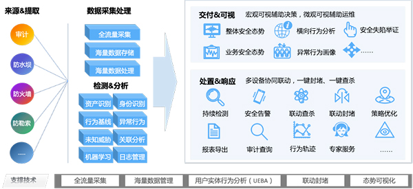
美创科技数据安全管理平台荣获2022数博会“领先科技成果奖”

Unity 游戏保护“大练兵”,一文读懂游戏事前防御

How does the beauty salon management system solve the three problems of store operation?

Why are the current membership warehouse stores bursting out collectively?

Flash framework web development video notes

8、原子操作类之18罗汉增强
随机推荐
7、CAS
Venue floor efficiency is so low? The key lies in these two aspects
Another way to achieve family reunion, 2022 flagship projection nut j10s is planted with grass
Record a JVM GC process
Installation and use of saltstack
秒杀中的验证码安全机制
4K投影仪哪款性价比最高,当贝X3 Pro高亮128G存储618值得看
Sulley fuzzer learning
Wireshark packet capturing and debugging RTSP
CMD of Jerry's AI protocol_ SET_ BT_ Name [chapter]
Redis數據類型日常使用場景
How to optimize SEO on the mobile terminal? Do you need to optimize GoogleSEO on the mobile terminal for a separate m domain name?
7、CAS
石头科技:研发实力和过硬品质 助力扫地机器人产业升级
Jerry's aicmd command [chapter]
Adobe Premiere基础-批量素材导入序列-变速和倒放(回忆)-连续动作镜头切换-字幕要求(十三)
Flip window join, interval join, window cogroup
STM32 development of practical series 7-data Porter DMA
Record a CODIS memory cleanup
2020.10.27 北京阿里大文娱一面总结