当前位置:网站首页>Briefly talk about the identification protocol of mobile port -bc1.2
Briefly talk about the identification protocol of mobile port -bc1.2
2022-07-05 08:10:00 【Learning notes of hardware Xiaobai】
About BC1.2 agreement Every engineer engaged in mobile phone hardware design should be very familiar with , It is mainly for the identification of charging port . However, about this part of the agreement , There are many explanations on the Internet , Someone said it very carefully , There are also very rough , Xiaobian is also to learn this part of the agreement , Read a lot of information , Finally, I decided to combine what I learned with what I really encountered at work to make some simple descriptions and explanations .
First of all, we need to know a few nouns
SDP:Standard Downstream Port Standard downlink port , For example, the computer USB mouth . The charging capacity of this port is 0.5A
CDP:Charging Downstream Port With strong charging capacity USB mouth , For example, the computer USB mouth . The charging capacity of this port is average 1.5A.
DCP: Dedicate Charging Port Special charging port , Like mobile phone chargers
PD:portable Device Portable devices , Such as mobile phone .
————————————————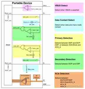 The figure shows the framework of charging port detection
The identification of charging port is mainly divided into the following five steps :
(1)VBUS Detect
(2)Data Contact Detect
(3)Primary Detection
(4)Secondary Detection
(5)ACA Detection
This article mainly talks about the first four common stages
VBUS testing
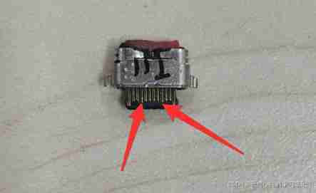
stay BC1.2 Before the start , First of all, it will be done VBUS Detection of . every last PD There is an in-phase comparator inside , Used to detect VBUS. When the adapter is connected PD when , Only the comparator VBUS Greater than the reference voltage VOTG_SESS_VLD when ,VBUS It will work , The following operations will be carried out . Additional explanation : Because the mobile port USB The design of the seat ( The arrow points to VBUS Pin ),TYPE C Terminal VBUS The pin first touches the mobile phone ( remove GND End ), Next is the data pin contact . This is why the charging identification process , The first thing to do is VBUS detect 了 .
DCD testing
Data Contact Detect, Data connection line detection , That is, judge whether the adapter is fully connected to the mobile phone USB Transposon .
End of judgment VBUS After access , Then it is to judge whether the connection of data signals is in place .
When Attached when
Mobile phone terminal D+ Of IDP_SRC open , because D+ A resistor is terminated RDP_DWN Go down to the ground , therefore D+ There will be a certain small voltage , When the voltage is less than the reference value , explain USB Good access . So look at the waveform D+ There is a very small voltage fluctuation at the front end .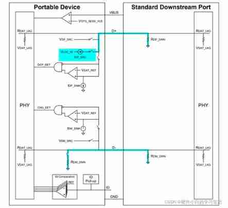
However DCD The detection of is not necessary , If not implemented DCD Detection of , The agreement will be in VBUS Effective T DCD_TIMEOUT Start the next steps ( The following waveform is not executed DCD Detection ).Charging port detection
(1) Primary Detection : distinguish SDP And DCP CDP
When PD Connect to SDP when ,PD The device will open the upper VDP_SRC With the middle IDM_SINK, the D+ There is a certain voltage ( Probably 0.6V), That is, the graphic waveform D+ stay “Primary detection” The higher part in . Then the mobile phone starts to detect D- The voltage of , When D- The voltage is less than VDAT_REF It is thought that what is recognized is SDP. When D- The voltage is greater than VDAT_REF, It is thought that what is recognized is DCP perhaps CDP, Then start the secondary detection .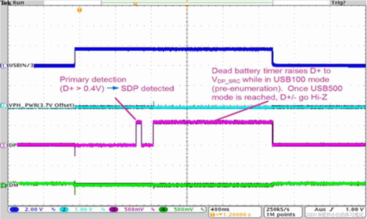 SDP
SDP
(2)Secondary Detection: distinguish DCP And CDP
CDP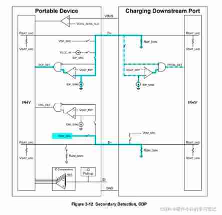
After the first test ,PD Will be in D- End open VDM_SRC, stay D+ End open IDP_SINK, At the same time, compare D+ The voltage at the terminal is the same as VDAT_REF, If it is less than VDAT_REF. It indicates that the connected device belongs to CDP.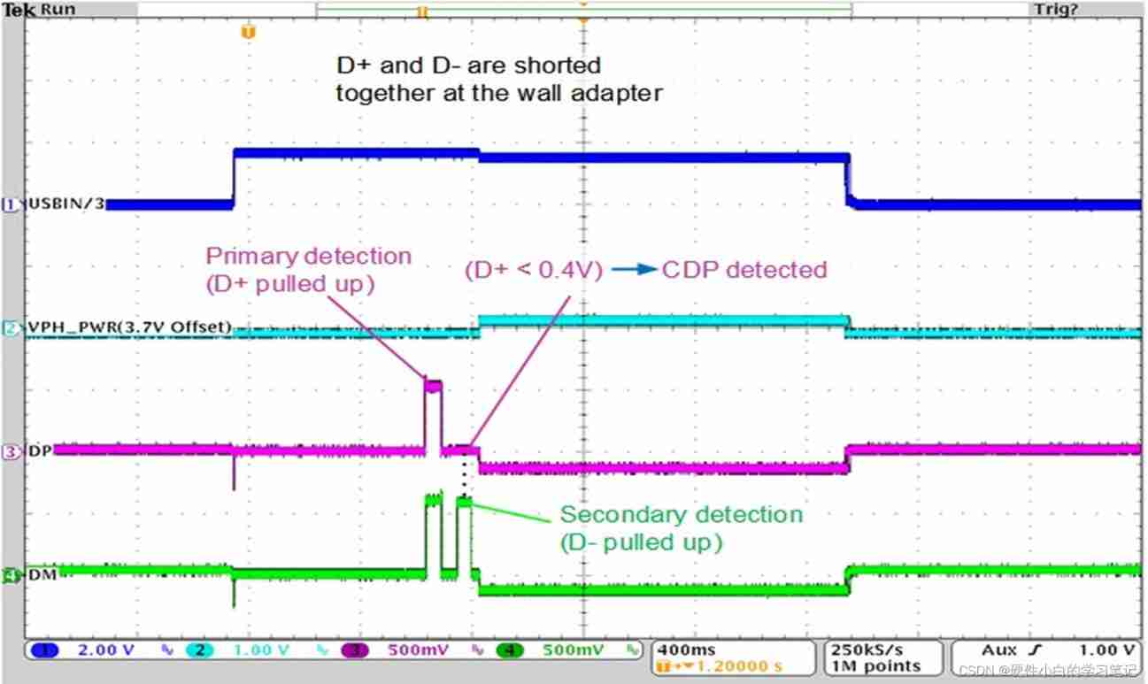
DCP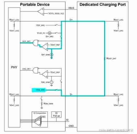
if D+ The voltage at the terminal is greater than VDAT_REF, It shows that the access is DCP, because D+ And D- Through between RDCP_DAT Short circuited together . therefore D+ And D- The voltage is almost similar .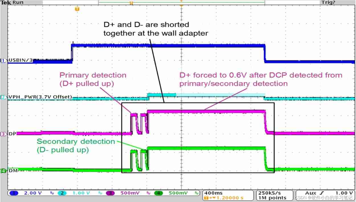
stay DCP After the test , We also need to check whether the protocol supports QC2.0. It will be in D+ End application 0.6V voltage , because DCP Stage ,D+ And D- Short circuited together , therefore D+ And D- The voltage is always the same . Is maintaining 1.25s after D+ And D- Will disconnect the short circuit , if D- The voltage drops to 0V And for a while , Description this adapter supports QC2.0.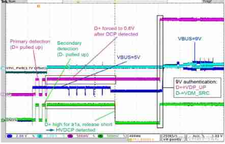
stay D- Fall to 0V And maintain it for a period of time ,D+ And D- The voltage continues to change , This is the picture D+ D- The last stage , It follows the following principles , Inform the charger , Output the corresponding voltage .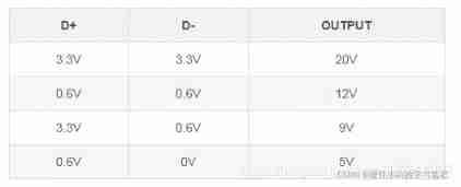
The waveform in the above figure :D+ Final 3.3V,D- Final 0.6V therefore VBUS Be raised to 9V.
All in all , Summarize according to the waveform , In the identification phase ,Primary Detect from D+ launch ,Secondary Detect from D- launch .SDP DCP CDP The difference between the three in waveform ,SDP stay Primary Detect Is recognized , All are located only once D+ High level of .DCP because D+ D- Short circuited by resistance , therefore D+ And D- Always maintain the same level , Both are in the high-level state .CDP It is seen as the waveform neutralization of the two ,D+ There is only one high level ,D- There are two high levels .
边栏推荐
- Soem EtherCAT source code analysis attachment 1 (establishment of communication operation environment)
- Gradle composite construction
- [tutorial 19 of trio basic from introduction to proficiency] detailed introduction of trio as a slave station connecting to the third-party bus (anybus PROFIBUS DP...)
- Measurement fitting based on Halcon learning [III] PM_ measure_ board. Hdev routine
- Circleq of linked list
- Factors affecting the quality of slip rings in production
- Makefile application
- UEFI development learning 6 - creation of protocol
- Matlab2018b problem solving when installing embedded coder support package for stmicroelectronic
- Altium designer learning (I)
猜你喜欢
Several important parameters of LDO circuit design and type selection
Management and use of DokuWiki

Consul installation
Management and use of DokuWiki (supplementary)

UEFI development learning 5 - simple use of protocol
![C WinForm [help interface - send email] - practice five](/img/2a/c4e7abe054e6fdd45acc7d297a033d.jpg)
C WinForm [help interface - send email] - practice five
Explain task scheduling based on Cortex-M3 in detail (Part 2)
Classic application of MOS transistor circuit design (2) - switch circuit design
C, Numerical Recipes in C, solution of linear algebraic equations, LU decomposition source program

List of linked lists
随机推荐
Soem EtherCAT source code analysis II (list of known configuration information)
Several important parameters of LDO circuit design and type selection
How to migrate the device data accessed by the RTSP of the easycvr platform to easynvr?
Programming knowledge -- assembly knowledge
H264 (I) i/p/b frame gop/idr/ and other parameters
Process communication mode between different hosts -- socket
Nb-iot technical summary
IEEE access personal contribution experience record
Gradle复合构建
Live555 push RTSP audio and video stream summary (I) cross compilation
Development tools -- gcc compiler usage
Classic application of MOS transistor circuit design (2) - switch circuit design
Basic embedded concepts
C WinForm [change the position of the form after running] - Practical Exercise 4
Pointnet++ classification practice
Correlation based template matching based on Halcon learning [II] find_ ncc_ model_ defocused_ precision. hdev
Record the opening ceremony of Beijing Winter Olympics with display equipment
Markdown tips
Gradle composite construction
Ble encryption details