当前位置:网站首页>Digital integrated circuit: CMOS inverter (I) static characteristics
Digital integrated circuit: CMOS inverter (I) static characteristics
2022-07-27 04:46:00 【Time Flies Fang】
Digital integrated circuit :CMOS Inverter ( One )
introduction
Inverter , seeing the name of a thing one thinks of its function , What it does logically is counterproductive , And in the CMOS In integrated circuit , The inverter consists of two complementary transistors NMOS+PMOS form , Inverter is also one of the most basic digital logic gates , Understand the characteristics of inverter , It is the basis for exploring more complex digital logic circuits , This section will start from CMOS Starting from the static characteristics of the inverter , To introduce the content of this part .
CMOS DC characteristics of inverter
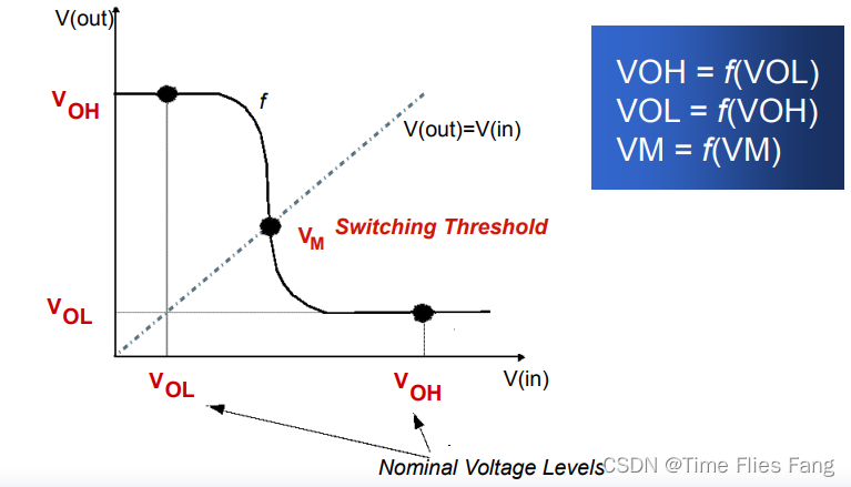
DC characteristics , Also known as voltage transfer characteristics , refer to CMOS When inverter is given different input voltage , When the steady state is reached , Value of output voltage , As shown in the figure below , In terms of logical function , We are all familiar with the inverter input high level to get low level , Input low level to get high level . But when we look at a real voltage transfer curve , We will find that when the input voltage is Vol and Voh Between time , There will be a smooth level switching process , How does this smooth curve come into being , And what is the specific working state of the two transistors behind this seemingly simple voltage transfer curve ?
CMOS Inverter structure and load characteristics
Here is a CMOS Typical schematic structure of inverter , Want to know how the inverter works , We have to go back to Digital integrated circuit : Device chapter ( One ) in , Explore the working area and voltage of the two transistors - Current transfer curve . But the problem is , To determine the working area of the transistor, you need to know Vgs, That is to say Vin outside , And we need to make sure Vds And Vgs-Vt The relationship between , and Vds What is unknown here Vout.
Regarding this , because NMOS and PMOS It's a serial relationship , The drain of the two tubes is conductive , therefore , We can go through NMOS and PMOS The voltage of - Current transfer curve , Through the graphic method, we can get the given Vin when , The intersection of the current transfer curves of two tubes , To get the output current value at this time , because PMOS The direction of the current curve follows NMOS contrary , So we need coordinate system mapping method to draw such a curve .
Through the above modeling process , We can finally draw the curve in the figure below , The curve in the figure below is different Vin Next NMOS and PMOS Intersection of current curve , That is, it forms the voltage transfer curve of the inverter .Vin from 0 Increase to Vdd, It has gone through the following five steps :
(1)N Pipe cut off ,P The tube is in the linear region , here Vin<Vt, Id≈0,PMOS The pull-up logic of will make Vout=Vdd;
(2)N Tube saturation ,P The tube is in the linear region , At this time, it is still in PMOS Strong pull up ,Vds The potential is high , about N In terms of Vds > Vgs - Vt;
(3)N Tube saturation ,P Tube saturation , At this time, it is in the region with the largest gain of the two tubes , But the logic level probability is in an unstable state ;
(4)N Pipeline ,P Tube saturation , At this time NMOS Strong pull-down , And (2) State symmetry ;
(5)N Pipeline ,P Pipe cut off , And (1) State symmetry .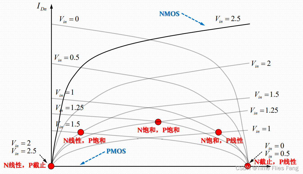
The relationship between DC characteristics and power supply voltage
hypothesis Vt=0.4V, In different Vdd Next , Draw the DC characteristics of the inverter , In the left half of the graph, it is consistent with our expectation , Maintain the opposite logical relationship , However, the right half of the figure shows the power supply voltage ratio Vt Another hour , The results show that the inverter can still decrease with the supply voltage , Keep the reverse logic unchanged for a long time . Maybe readers have questions , Mingming Vdd<Vt, That is, in any case, both tubes are in the cut-off state , It has not been opened , Why can we keep the function correct ?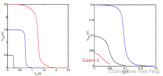
The answer is because Leakage current The existence of , The phenomenon of leakage will also be analyzed in more detail in the subsequent articles on power consumption analysis . In short , Even if the transistor is in the off state , There will also be current from source to drain , And it can be controlled by the grid voltage .Vdd An inverter in a state below the threshold is called Deep sub threshold (Subthreshold) Inverter , This is also one of the methods often used in low-power design .
Relationship between DC characteristics and process fluctuation
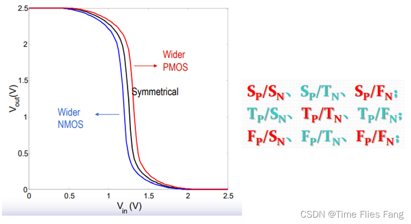
In the actual manufacturing process of transistors , Process deviation is inevitable , Due to the difference of doping concentration , Or the difference of channel width , Will affect the speed of a transistor . For example , High doping concentration MOS The threshold voltage of the tube is lower , Can be opened faster , The transistor with wider channel width has stronger driving ability of current, and so on . These performance impacts caused by process fluctuations can be concentrated in the inverter , For example, as shown in the figure below , When N Well done ,P When it's done badly , because N The tube driving ability becomes stronger , Switch threshold Vm Will become lower , On the contrary, it will become higher . In order to better overcome the timing deviation caused by process fluctuation , In simulation , We use it corner, That is, the simulation of boundary value , To simulate the transistor process limit angle as comprehensively as possible . The right side of the figure below shows four corner And a typical Of case, It's fast and slow PMOS Tube and NMOS Arrangement and combination of tubes . This is also the time series analysis run in the digital backend ss, tt, ff etc. corner The meaning of .
边栏推荐
- Visualization domain svg
- Pinia uses plug-ins for persistent storage.
- Use the kubesphere graphical interface dashboard to enable the Devops function
- iPhone13再降价,其实只是做做样子,消费者都在等iPhone14
- Network knowledge corner | it only takes four steps to teach you to use SecureCRT to connect to ENSP. You must see the operation guide of common tools
- 冒泡排序(详细)
- Ffmpeg merge video function
- From scratch, C language intensive Lecture 4: array
- Structural mode - facade mode
- The project parameters are made into configurable items, and the @configurationproperties annotation is used
猜你喜欢
Head detached from origin/... Causes push failure

Influxdb basic understanding

IIC 通信协议 (一)

Install and configure Debian on a wired network

Overview of communication protocols

Session&Cookie&token

The data in echart histogram is displayed at the top of the chart
![Shell中的文本处理工具、cut [选项参数] filename 说明:默认分隔符是制表符、awk [选项参数] ‘/pattern1/{action1}filename 、awk 的内置变量](/img/ed/941276a15d1c4ab67d397fb3286022.png)
Shell中的文本处理工具、cut [选项参数] filename 说明:默认分隔符是制表符、awk [选项参数] ‘/pattern1/{action1}filename 、awk 的内置变量

JS modify the key value of the object array
可视化领域 SVG
随机推荐
Okaleido tiger will log in to binance NFT in the second round, or continue to create sales achievements
【独立站建设】跨境电商出海开网店,首选这个网站建设!
Dino paper accuracy, and analyze the variant of its model structure & Detr
RSA 非对称 加密解密 加签验签工具
Yolov4 network details
Chapter 4 scope and life cycle of bean object
ros 相机标定 sensor_msgs/CameraInfo Message 数据类型及含义
Easy to use shell shortcuts
0 dynamic programming medium leetcode467. The only substring in the surrounding string
How can I index the Oracle database field date?
Shell中的文本处理工具、cut [选项参数] filename 说明:默认分隔符是制表符、awk [选项参数] ‘/pattern1/{action1}filename 、awk 的内置变量
Scala immutable map, variable map, map conversion to other data types
干货 | 独立站运营怎么提高在线聊天客户服务?
Nacos startup and login
Unity:Resource Merging、Static Batching、Dynamic Batching、GPU Instancing
第六章:云数据库
数组中的最大值,最小值,冒泡排序
结构型模式-桥接模式
How to set user-defined display for Jiaming Watch
Structural mode - facade mode