This is a IC The first in the history of men's struggle 11 Original article
Official account 「IC Male struggle history 」, Let's roll up our sleeves and work hard !
this paper 1892 word , Expected reading 5 minute .
today , Jacko shows you how to turn sand into chips , Help zero basic Xiaobai quickly understand the chip manufacturing process .
1 Wafer manufacturing
The original raw material of the chip on the tall is actually sand , This is also the magic place of science and Technology . The main component of sand is silica (SiO2), The deoxidized sand contains at most 25% The silicon element , Silicon is the second most abundant element in the earth's crust , This is also the foundation of semiconductor manufacturing industry .
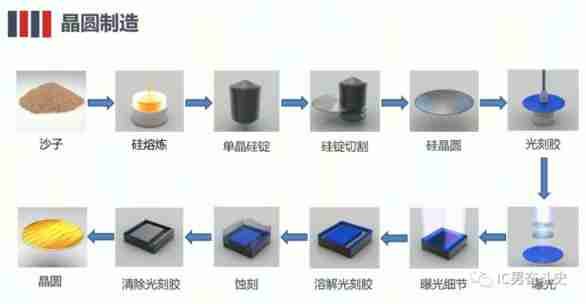
High purity polycrystalline silicon for semiconductor manufacturing can be obtained by melting sand and multi-step purification and purification , Scientific name: electronic grade silicon , On average, there is at most one impurity atom per million silicon atoms .24K Kim, everyone knows , Gold purity up to 99.998%, But still not as pure as this electronic grade silicon .
Put the high-purity polysilicon in the single crystal furnace to draw , You can get a nearly cylindrical monocrystalline silicon ingot , Weight approx 100 kg , The purity of silicon is up to 99.9999% above . Then cut the monocrystalline silicon ingot laterally into a circular single silicon wafer , You get a monocrystalline silicon wafer , This is what we often call the wafer used to make chips (Wafer).
Monocrystalline silicon is better than polycrystalline silicon in electrical and mechanical properties , Therefore, semiconductor manufacturing is based on monocrystalline silicon .
Let me give you an example from life , It can help you understand polysilicon and monocrystalline silicon . Rock sugar everyone should have seen , When I was a child, I often ate rock candy like small square ice cubes , It's actually crystal rock sugar . Correspondingly, there are also polycrystalline rock sugar , The shape is usually irregular , Used to make traditional Chinese medicine or make soup , It has the effect of moistening lung and relieving cough .
The crystal arrangement structure of the same substance is different , Its performance and use will also be different , Even the difference is obvious .
Semiconductor manufacturing enterprises , Intel, for example 、 Factories such as TSMC and SMIC usually do not produce wafers , Just a wafer Porter , from Wafer Buy directly from suppliers .
Wafer manufacturing is to put the designed circuit ( The technical term is mask , The English name is Mask) On a wafer .
First, we need to put the photoresist (Photo Resist) Evenly spread on the wafer surface , In this process, you need to keep the wafer rotating , This allows the photoresist to be laid very thin 、 Very flat . Then the photoresist layer passes through the mask (Mask) Exposed to ultraviolet light (UV) under , Become soluble .
The mask is printed with a pre designed circuit pattern , Ultraviolet rays shine through it on the photoresist layer , Will form every layer of the circuit pattern . Generally speaking , The circuit pattern obtained on the wafer is a quarter of the pattern on the mask .
The next step is to dissolve the photoresist , The photoresist exposed to ultraviolet light is dissolved by chemical reagent , The pattern left after removal is consistent with that on the mask . Then etching , Use chemicals to dissolve the exposed parts of the wafer , The rest of the photoresist protects the parts that should not be etched . After etching , The mission of photoresist is completed , After all are cleared, you can see the designed circuit pattern . This series of processes we call lithography .
The process of lithography is actually similar to the process of taking pictures with a fool's camera in our life . The wafer covered with photoresist is the film of the camera , The real thing we want to shoot is the mask , The process of photographing is the process of semiconductor exposure , The process of developing film is similar to subsequent etching and dissolving photoresist .
The final result is somewhat similar , Lithography realizes the designed circuit on the wafer , Got the chip , Like taking pictures, the appearance of the real object is realized on the film , Got the picture .
Lithography is one of the most important processes in chip manufacturing . By lithography , We have realized that the designed circuit is laid on the wafer , By repeating, multiple identical circuits can be realized on the wafer , Each circuit is a separate chip , English is called die. The actual chip manufacturing process is much more complicated than this , It usually takes hundreds of processes . So semiconductors are the crown of manufacturing .
Understanding the chip manufacturing process is very important for the posts related to semiconductor manufacturing , In especial FAB The factory is like TSMC 、 Technicians from SMIC and other factories , Or mass production related positions in the chip R & D team, such as product engineer 、 Test engineer, etc , All belong to the necessary basic knowledge .
2 CP test
CP yes Chip Probing Abbreviation ,CP Testing belongs to wafer level testing , Through the probe card (Probe Card) And probe table (Prober) Make automated test equipment (ATE,Automatic Test Equipment) To a single chip on a wafer (die) Establish electrical connection between .CP The purpose of the test is to ensure that each die Can meet the design specifications of the chip (Specification), Sift out those with problems die, Then do chip packaging . This can reduce the cost of chip packaging , At the same time, ensure the quality of the chip .

CP The hardware equipment required for the test includes probe card 、 Probe table 、ATE The tester and the interface between the tester and the probe card (Mechanical Interface).
Test engineers need to be based on ATE Test platform development CP The test program , The content usually includes electrical connectivity test 、 Function test and parameter test, etc .CP The test program will be based on the test results Pass perhaps Fail Score Bin And generate Inkless Map, Mark the test Fail die Of wafer map chart .
CP The test results are usually counted in the form of yield , Yield means pass die Take up the test die Percentage of total . Corresponding , Yield loss refers to fail die Take up the test die Percentage of total .CP Testing is also called intermediate testing , It is the first stop of semiconductor back channel packaging test , It is also the first test to verify the chip design specification after chip manufacturing .
From the perspective of saving chip production cost , We should put as many test items as possible into CP In the test , Improve CP Test coverage , Sift out faulty chips as early as possible . But accordingly ,CP The cost of testing hardware ( Mainly probe card and testing machine ) It will also rise , In the final analysis, it is actually a compromise problem .
If the chip market demand is relatively large , The cost of testing hardware is insignificant compared with the profit from sales , Then we should try to improve CP Test coverage . conversely , You need to consider saving hardware costs .
understand CP Testing is very important for the post related to semiconductor packaging testing , In particular, the sealing and testing factory is like the sun and moonlight 、 Depend on 、 Changdian, etc CP Test related technicians , Or mass production related positions in the chip R & D team, such as product engineer 、 Test engineer, etc , All belong to the necessary basic knowledge .
To be continued …... Tomorrow, 21:00 Publish a sequel .
At the end of the text, scan the code and add Jiege wechat , Provide all kinds of semiconductor industry research reports free of charge :
END
Official account 「IC Male struggle history 」, Let's roll up our sleeves and work hard !

● third time “ World War ”—— Chip defense war , Smokeless battlefield !
● Series ( Next ): This is our golden age
● Series ( On ): Core shortage , Where is the road of automobile chip
● Chip engineers are too expensive , Your sister !