当前位置:网站首页>FPGA (III) trigger and latch
FPGA (III) trigger and latch
2022-06-12 15:28:00 【Jian Chen~】
List of articles
Preface
In most digital systems , In addition to the combinational logic circuit with logic operation and arithmetic operation functions , A circuit with storage function is also required . Combinational circuit and memory circuit are combined to form sequential logic circuit , Sequential circuit for short . This chapter mainly discusses two kinds of logic unit circuits to realize the storage function : Latches and triggers .One 、 Basic bistable circuit
According to my digital book , Various latches and triggers , Are based on basic bistable circuits , therefore , First, let's talk about it in general Basic bistable circuit .
The basic bistable circuit consists of two non gates G1 and G2 It is connected in the form of cross coupling as shown in the figure below .
- Q Set up 1, that Q’=0. This is called the basic bistable circuit 1 state
- Q Set up 0, that Q’=1. This is called the basic bistable circuit 0 state
The circuit has 1 and 0 Two kinds of state , Once in one of these States , It can remain unchanged for a long time . So it is also called Bistable memory circuit .
The function of bistable circuit is extremely incomplete . After the power is turned on , It may enter at random 1 State or 0 state , Because there is no control mechanism , Therefore, it is impossible to change and control its state during operation , Therefore, it can not be used as a storage circuit .( That is, it is not practical 、 reliability )
Two 、 Latch
1. Or not SR Latch
The NOR gate of a basic bistable circuit is replaced by a NOR gate , Then it constitutes the basic SR Latch , It is a bistable circuit with the simplest control function . Compared with the basic bistable circuit ,SR The latch has two inputs S and R. In digital circuits ,“S” Generally speaking “Set”( High active ),“R” Express “Reset”( Low level active ).
Menu by :
Through the analysis of the menu , To ensure that the latch is always in the defined state , The input signal shall comply with SR=0 Of constraint condition , That is, not allowed S=R=1 .
Working waveform by :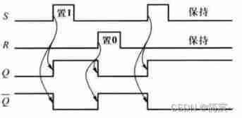
At that time , There is no such thing as S=R=1 after ,SR The latch goes into an indeterminate state . If S or R There is one party to set first 1, The other is a little behind 1, be Q or Q’ One of them will be in S and R All set 1 when , Set as 0. If S and R Of 1 level Different time revoke , After that, the output state can still be determined , As shown in the figure below ③ and ④ Shown :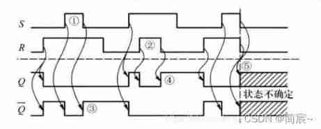
2. NAND gate SR Latch
Actually , There are more than NAND gates SR Latch , There is also a basic or non gate structure SR Latch .

3. D Latch
And SR Latches are different ,D The latch has no undefined state in operation , Therefore, it has been widely used . at present ,CMOS The integrated circuit mainly adopts transmission gating D Latches and logic gating D The latch has two circuit structures , In particular, the circuit structure of the former is simple 、 It takes up a small area in the chip and is more popular .
① Transmission gating D Latch
Two transmission gates are inserted into the basic bistable circuit TG1 and TG2, The following transmission gating can be formed D Latch .
Menu by :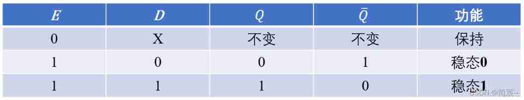
② Logic gating D Latch
Logic gating D The latch is in the door control SR The latch's S and R A not gate is connected between the inputs G5, So as to ensure SR=0 Constraints of , Eliminates possible undefined States .

3、 ... and 、 trigger
A latch is a pulse level sensitive memory cell . The most important feature is the enabling latch level function , That is, when the enable signal is valid , The output signal can be locked and kept unchanged , When the enable signal fails , The output is the same as the input , Equivalent to an output buffer .
Flip flops are also called bistable flip flops , As the input changes , The output will change accordingly . It is usually a feedback combinational logic circuit composed of at least two identical gates . In order to make the triggering process easy to control , And make the timing logic circuit controlled by the clock trigger .
Common are SR trigger ,D trigger ,JK trigger . Triggers usually have two states , Conserved state and transformed state , Corresponding to two input conditions respectively , In the hold state, the output will remain in the current state , In the transformed state, the output will change in a regular order .
There is a paragraph in the digital book , The difference between trigger and latch is roughly described , It also gives a simple definition of trigger :
As mentioned earlier D Latch , Its output will change with the input signal . Many sequential circuits require that the memory circuit is only sensitive to the rising or falling edge of the clock signal , At other times, it stays the same .( The first two sentences are different ) This state update, which is sensitive to the edge of the clock pulse, is called Trigger , A storage unit having a trigger operating characteristic becomes trigger .( The setting of the trigger ) Flip flops with different circuit structures may have different sensitive edges to clock pulses , It is divided into rising edge trigger and falling edge trigger .
At present, there are three kinds of circuit structures for flip flops : Master slave trigger 、 Maintain blocking trigger and Trigger using transmission delay .
1. Master-slave D trigger
Put two D Latch cascading , It constitutes a typical COMS Master-slave D trigger , The latch on the left is called Main latch , The one on the right is called From the latch , The enabling signals of the master and the slave are in opposite phases , Use the interactive latch of two latches , The isolation between the stored data and the input signal can be realized .
The following figure CP Represents a clock signal .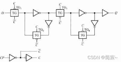
The analysis process is as follows :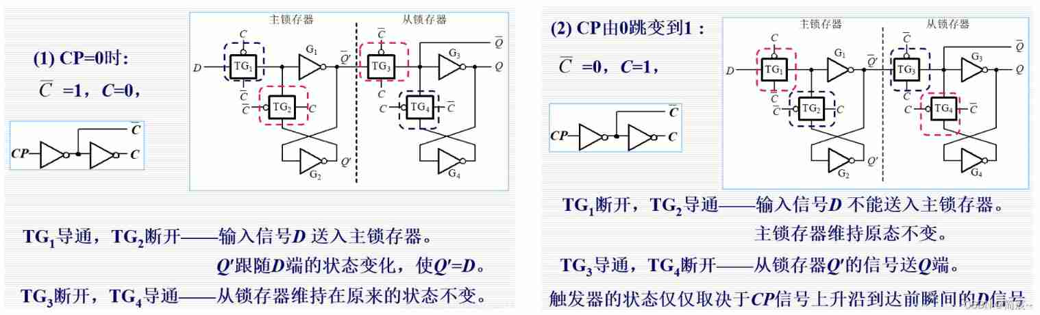

2. Logic function of trigger
The state of the trigger before the arrival of each clock trigger edge is called Initial state , The subsequent state is called Substate . The logic function of the so-called trigger , It refers to taking the input signal and current state as variables , A logical relation with a substate as a function , You can use the property table 、 Characteristic equation or state diagram to describe this relationship . According to the logic function of the trigger , Usually divided into D trigger 、JK trigger 、T Trigger and SR Several different types of triggers .
Logic function and circuit structure are two different concepts . The trigger of a certain logic function can be realized with different circuit structures , meanwhile , Based on a basic circuit structure , It can also form triggers with different logic functions .
①D trigger
D The next state and input of the trigger D identical , It has nothing to do with the previous state .
②JK trigger
In all logic type triggers ,JK The trigger has the strongest logic function , On the outside J、K Under signal control , It can perform hold 、 Set up 0、 Set up 1 And flip , And it can be converted into trigger with other functions by simple additional circuit .
③T trigger
In some applications , Some technical functions need to be controlled : When the control signal T=1 when , Every one of them CP pulse ( Clock cycle ), Its state is reversed once ; And when T=0 when , It's not right CP The signal makes corresponding and keeps the state unchanged .
④T’ trigger
When T Trigger T When the input terminal is fixed to the high level ( namely T=1), Then every time the clock pulse acts , The trigger flips once . This particular T Flip flops often appear in the internal logic diagrams of integrated circuits , Its input is only clock signal , Sometimes called T’ trigger .
⑤SR trigger
Only set 、 The trigger of the reset function is called SR trigger .S=R=1 when , The secondary state of a trigger is indeterminate , If that happens , The trigger will lose control , therefore ,SR The use of triggers must follow SR=0 Constraints of .
Four 、 use Verilog Describe latches and triggers
stay Verilog in , The sensitive events in the logic level are divided into two types : Level sensitive events and edge triggered events .① In Combinational Circuits , The change of input signal will directly lead to the change of output signal ;② The output of the latch in the sequential circuit also changes with the input level when the enable signal is high .
① Combinational logic circuit :
always @(*) 		// or
always @(D,S) 	// among D、S Is the signal
② Sequential circuits :
always @(posedge clk or negedge rstn) // among clk For the clock signal ,rstn It's a reset signal
stay IEEE 1364-1995 In the standard , Require keywords between multiple events or Connect , The modified standard can separate multiple asynchronous events with commas .
1. D Latch behavior level description
about D For latches , When the input control signal is at the effective level ( namely E=1), Its output Q Follow the input signal D The change of ; When the control signal is invalid , Output Q remain unchanged .
module D_latch (
    input           D       ,// Port declaration , Input signal
    input           E       ,// Control signals

    output reg      Q       ,
    output          QN
);
assign  QN = ~Q;
always @(E or D) begin
    if(E)
        Q <= D;
end
endmodule
2. basic D Trigger behavior level description
At the rising edge of the clock signal , The input signal D The value is assigned to Q, At any other time , No matter what D How the signal changes , Can't change Q The state of .
module DFF (
    input       clk     ,// The system clock
    input       D       ,// Input signal

    output reg  Q        // The output signal
);
always @(posedge clk) begin
    Q <= D;
end

endmodule
3. JK Trigger behavior level description
according to JK Characteristic table of trigger , Use case Statement to describe . Will enter the variable J、K Concatenated into a binary variable ({J,K}).
module JK_FF (
    input           clk         ,
    input           J,K         ,
    output          QN          ,
    output reg      Q
);
assign QN = ~Q;
always @(negedge clk) begin
    case ({
    J,K})
        2'b00:Q <= Q;       // The state remains the same
        2'b01:Q <= 1'b0;    // Set up 0
        2'b10:Q <= 1'b1;    // Set up 1
        2'b11:Q <= ~Q;      // Flip
        default: ;
    endcase
end
endmodule
Reference resources
Fundamentals of digital electronic technology 5—— Latch and trigger It is equivalent to giving the contents of this section in the digital book to “ Carry ” Over here. , Although there are some defects in this picture , But it's still pretty good .
Fundamentals of digital electricity (5)– Latches and triggers It's kind of like what the digital teacher said in class PPT, Let's talk about the whole chapter .
The difference between a latch and a trigger It's a big guy's summary of the difference , It's simple but essential , It is attached with Verilog Write D trigger 、T trigger 、JK Trigger tutorial .
In digital circuits D Trigger and D What are the functions of the latches ? use 6 Methods , They are the textual narration of functions 、 Menu 、 State transition truth table 、 Characteristic equation 、 State diagram 、 The sequence diagram summarily introduces D Trigger and D Latch .
边栏推荐
- Socket原理讲解(在哪、是什么、怎么用)
- Error 1105: message:\“raft entry is too large
- CUDA out of memory 或 BrokenPipeError: [Errno 32] Broken pipe 或 OSError: [WinError 1455] 页面文件太小的解决办法
- Left aligned, right aligned, random number, goto, compare output bool
- Solving multithreading security problems
- Qiming Zhixian shares the application scheme of 2.8-inch handheld central control screen
- FIRST集与FOLLOW集白话版
- Remote control of other computers -- detailed tutorial
- Seaborn Brief
- Deepin20.6 rtx3080 installer le lecteur de carte graphique 510.60.02, cuda 11.6, pytorch1.11
猜你喜欢


随机推荐
Village to village communication (and collective search)
Swap numbers, XOR, operator correlation
Use and understanding of generics
Idea pull branch code
Acwing暑期每日一题(6月10日性感素数)
Is it safe to open an account for flush mobile stock trading
Multi thread knowledge induction
UDP总结(TCP/IP详解卷1/2)
Mh32f103arpt6 hardware and software compatible alternative to stm32f103rct6
RARP summary (tcp/ip explanation volume 1/2)
Ngork implements intranet penetration -- free
【光源实用案例】 UV-LED固化创新,让产线变得更丝滑
Qiming cloud sharing | demonstrate the switch through an example of the matter protocol to control the light on and off through the matter protocol
Function recursion example
Acwing summer daily question (sexy prime number on June 10)
jupyter notebook新环境快捷方式
Using the CSDN markdown editor
TCP与UDP的区别,以及TCP的三次握手和TCP的四次挥手
Use of boost:: bind() in ROS
Idea大全(转载)