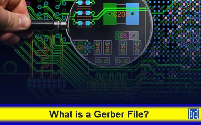
What is? Gerber file ?
Gerber Are we in PCB File formats often used in the industry . We use Gerber Document to describe PCB The various elements and components of the board . therefore , This includes legend layers , The metal we are going to use , Conductor layer , Wiring pad , And the solder mask . Gerber The format is provided by a company named Gerber The company developed and mainstreamed , Hence the name .
We use a special set of tools to design PCB plate . therefore , These tools mainly include CAD ( Computer aided design ) and EDA ( Electronic design automation ). These tools can help us generate basic PCB Manufacturing data . then , Based on these data, we started to make PCB. If the customer does not include Gerber In the case of a file PCB Design documents shall be provided to the manufacturer , Then the manufacturer will face many difficulties . This is because Gerber The file extension is PCB Manufacturing experience , Because it serves as a set of guidelines and references .. Manufacturers rely on PCB Gerber Viewer to describe and understand PCB Design parameters of various modules of the board . therefore , We can use Gerber Document carried out PCB Manufacture and assembly of .

Gerber What is the importance of documents ?
If you want to execute PCB manufacture , Must be used throughout the process Gerber file . On-line Gerber The file viewer is the standard for photographic plotters , Legend printer , CAD The designer , Image Analyst (AOI and X ray ), And multi tier manufacturers . therefore , The Gerber file is similar to the guide star , In the whole PCB Help the manufacturer in the manufacturing process .
Processing PCB When assembling , We are Gerber PCB Contains a template layer . This also enables us to adjust the position of various electronic components . therefore , It provides us with important data , For us SMT And through-hole assembly process .
Gerber File What are the different versions ??
Gerber File formats have been evolving , So there were many versions in the past . However , today , We mainly use three popular Gerber Document version .
1) Gerber X2
This is the latest free Gerber Viewer format . The best thing about this version is that it supports stack data . Besides , It also contains many advanced properties .
2) RS-274-X
This version of the PCB Gerber The file has the most extended functions . therefore , We're on a daily basis PCB This version is widely used in document viewer online manufacturing operations .
3) RS-274-D
This version of online Gerber The viewer format is one of the earliest , Most traditional PCB Manufacturers are still using it . However , Two other versions are gradually replacing this version .
Gerber File type and format
1) pcbname.GTL
We use this file type to store data related to the top copper layer .
2) pcbname.GTS
We often use this file type to store data related to the top solder mask .
3) pcbname.GTO
We are often in the routine PCB This type of file is used in manufacturing operations to store data related to top-level silk screen printing .
4) pcbname.GBL
majority PCB Manufacturers use this type of file in their settings to store information and data related to the underlying copper layer ..
5) pcbname.GBS
This format is best used to store information and details about the bottom solder mask .
6) pcbname.GBO
This format is very suitable for recording information related to bottom screen printing .
7) pcbname.TXT
We mainly use this file type or format to maintain records of drilling information . This mainly relates to PCB Data relating to holes and other features drilled in slabs .
8) pcbname.GML / GKO
This file format is best for storing and PCB Information about the board profile .
9) pcbname.GL2
We are only in multi-layer PCB This type of file is used in the board . It provides us with information about the second inner layer .
10) pcbname.GL3
This type of file is also reserved only for multi tier PCB plate . We use it to store information about the third inner layer .
How to go from Eagle Generate Gerber file ?
Autodesk Eagle Is used for PCB A very convenient tool for design and layout . It has scripting capabilities , Enables us to automate the electronic design process . stay Autodesk Eagle Finish in PCB After the design of the board , The next step is to generate Gerber file . This is because you have to put this Gerber File samples are sent to... Along with other design documents PCB Manufacturer . About Autodesk Eagle One of the best things about is that it contains a very intuitive CAM processor . This module enables us to import any CAM file , Then immediately generate PCB Any type of file that the board may need . therefore , You can use this feature to generate the required Gerber file .
1) open CAM processor

First , You must be in Autodesk Eagle Import and open PCB Layout file .. PCB The layout file has a (.brd) expand . therefore , To open it , You can click CAM Button . perhaps , You can do this in the following ways : First click “ file ”, Then navigate to CAM processor . Doing so will immediately open the for generation Gerber Of documents CAM processor ..
2) Navigate to work

The next step is to navigate to work . You can do this by clicking “ file ”, And then click “ open ” To perform this operation . Then switch the job button .
2) open gerb274x.cam file
You must first navigate to Autodesk Eagle Default CAM Folder .. therefore , From there you can choose gerb274x.cam file . After completion ,, You can choose to open .
3) Add a second screen print
If you browse Autodesk Eagle Tabs in , You will find that there are no documents in the bottom silk screen layer . This is because , If it's simple PCB plate , We usually only put screen printing on the top layer . However , If you have complex PCB, And add other screen printing on the bottom layer , Then you can do it too .
- First , You will have to click Add .
- then , You will have to change this section . You can use any relevant term , for example “ At the bottom of the screen ”
- after , You will have to fie Change to “%N.pls”
- then , You will have to deselect all layers
- Then select these layers : 26 “ bNames, 20 “ Size , and 22 “ bPlace”
4) Create a Gerber file

Now? , You can finally create what you need Gerber The file . For this purpose , You will have to click “ Processing jobs ” Button . then , You will Eagle See the desired... In the project folder of the control panel Gerber file ..
5) take Gerber File sent to MOKOTechnology
Generate Gerber After the document , You must send them to MOKO Technology, So that we can start processing your order . For this purpose , You will have to put all Gerber Put the files together and compress them into a folder . then , You can put this zip File upload to MOKO Technology Order page for . This will enable us to receive Gerber Documentation and your order description . therefore , We will begin our research immediately .
Common errors in Eagle Gerber files and their solutions
1) Missing drillthrough file
We need these documents to make sure that we want to PCB Location and size of holes drilled in the plate . If you forget to include these files , So your PCB Manufacturers will face great difficulties .
2) Lack of solder mask
If your PCB The board has two or more layers , The document must have two layers of solder mask . One for the top floor , The other is for the bottom layer .
3) Missing or repeated contour
One of the most common errors is that people often generate files with missing outlines . These profiles are important for determining where to cut PCB The board is very important . Sometimes people generate files by mistake , These documents are PCB There are two or more frames around the board . In both cases , PCB Manufacturers may face serious problems .
4) PCB Size mismatch
Usually , Enter... In order PCB The plate size is the same as that in Gerber The size entered in the file does not match . You should avoid using , So that we can prevent PCB Any significant delay in the manufacturing process .
5) Cut into the hole in the hole
Sometimes people place drill holes by mistake , So as to interfere with the circuit tracking . most important of all , They forgot to reposition the track around the hole . You should avoid this situation , So as not to damage PCB Functions of the board .
6) Gerber Plated and non plated holes are not clearly defined in the document
Sometimes people think about Gerber PCB How software distinguishes NPTH and PTH Lack of basic understanding . stay Autodesk Eagle in , You can use the hole tool to make NPTH. On the other hand , You must use “ adopt ” Tools to make PTH.
Last , To share a useful gerber Open source library ,hsiang-lee/gerber-parser: gerber-parser is an open source library for parsing and rendering gerber file. It uses qt painting system by default and you can save to any image format Qt supports, including jpg,png,bmg,svg,pdf and etc. Also, you can write your own rendering engine easily, if you don't want to use Qt. If you need more help, please contact me. (github.com)