当前位置:网站首页>II Stm32f407 chip GPIO programming, register operation, library function operation and bit segment operation
II Stm32f407 chip GPIO programming, register operation, library function operation and bit segment operation
2022-07-02 11:15:00 【Heavy vehicle water】
Stm32f407 chip GPIO Programming
GPIO It's called general input and output interface , As a general input and output function , Input and output 0 and 1, In high level 1, Low level means 0. stay ARM in , The high level is 3.3v, The low level is 0v.
1. View the downloaded schematic , It should be noted that , Pins with the same schematic name are physically connected , You can search the name of silk screen in principle to find the corresponding schematic diagram of hardware .
LED Schematic diagram corresponding to hardware

STM32 Schematic diagram corresponding to the chip


see LED Schematic diagram should achieve two purposes ( Connect or not VDD3v3 Situation judgment )
(1) Make clear the working mode of the operating hardware ( Combined with the instruction manual of hardware )
The corresponding pin is low ——LED bright
The corresponding pin is high ——LED destroy
(2) The hardware to operate is connected to CPU Those pins
D1——————PF9
D2——————PF10
D3——————PE13
D4——————PE14
see CPU The chip manual (STM32F4xx Chinese reference manual and Cortex-M4 Authoritative guide ) Hardware control is achieved by operating registers . There are three register configuration methods ,GPIO Register bit operation , Library function operation , Bit segment operation , The following will be introduced separately .
———————————————————————————————————————————
———————————————————————————————————————————
GPIO Register bit operation
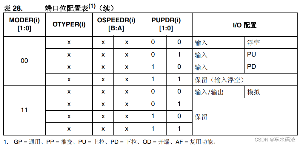
(1)GPIO I / O selection
Input ———— Floating space , On / Drop down input , Reuse , simulation
Output ———— push-pull / Open a leak , On / The drop-down , Reuse , simulation
The difference between push-pull and open drain : Push pull is to pull up , Opening a leak is a weak pull up , Opening the drain and raising the resistance requires external pull-up , Leakage opening also has the function of absorbing current , Can do two-way IO
(2) Output speed
low —— in —— high —— fast
(3) Locking mechanism
lock GPIO Configuration of
(4) Data register
Input data register ———— obtain GPIO Input level
Output data register Set up / Reset register ———— Set up GPIO Output level
(5) Function reuse options
Select multiplexing register
(6) Configuration register
Look up the table to determine the value of register configuration

Check the corresponding hardware register
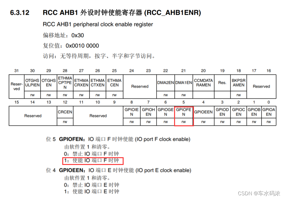
Stm32f407 share 9 Group GPIO(A~I), Each group 16 individual (0~15),stm32 All registers are 32 Bit .
Check the information you need to get from the hardware register
1. Get the address of the hardware register
stm32 The address of the register in uses the base address + The offset
The base address is in the reference manual 2.3 Query in the table of section
such as GPIOF The base address of the register =0x40021400, If there is an offset, add the offset
The offset of each register is on the description of the register
2. The contents represented by each bit of the register
———————————————————————————————————————————
———————————————————————————————————————————
Do a simple exercise
To configure PF9 The register is General push-pull output , No up and down , High speed output
Mode register
Base address = 0x40021400
(7) Configuration mode register

Bit operation configuration , More trouble
Volatile unsigned int *pxx = (unsigned int*)0x40021400;
// take 18~19 Bit is set to 01
*pxx &=~(0x3<<18); // Bits and operations , First the 18~19 Bit is set to 00
*pxx |=~(0x1<<18); // Bitwise OR operation , then 18~19 Bit is set to 01
Configure the output type register

Configure the output speed register

Pull up and down to select register

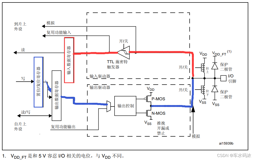
Through the above 4 The configuration of registers is completed PF9 The initialization , General push-pull output , No up and down , Fast output , The following is through reset / The set register controls the level of the output .
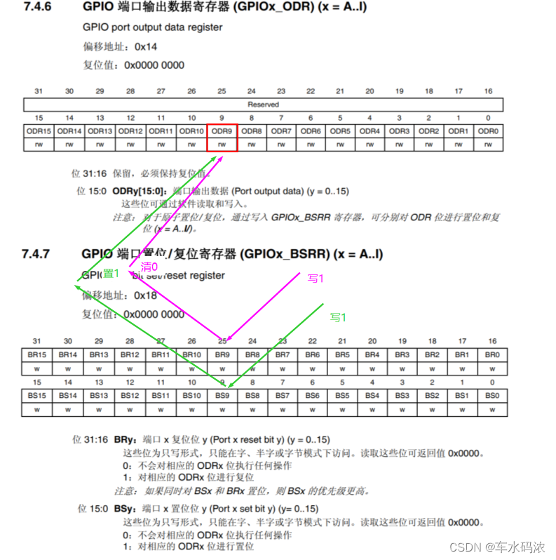
Here through configuration GPIO Set up / Reset register To control GPIO Output register Output level of , To configure PF9 register , The working principle we need to understand is ( Please look carefully at the register configuration matching relationship in the above figure , This is very important ):
The first point : Set the reset register BS9 Write in bit 1, Output register ODR9 The position will be set 1, Set the reset register BS9 Write in bit 0, Output register ODR9 The position will not change ;
Second point : Set the reset register BR9 Write in bit 1, Output register ODR9 The position will be cleared 0, Set the reset register BR9 Write in bit 0, Output register ODR9 The position will not change ; This is through GPIO Set up / Reset register control GPIO Method of outputting the output level of the register .
to want to GPIO Normal work , Must be turned on GPIO Clock switch , Configure through the peripheral clock enable register
Base address :0x40023800
Write drivers
Stm32 The macro definition of register address is officially provided , You can use it directly .
The idea of writing code ( Pseudo code )
- initialization
Start GPIO The clock
take PF9 Configured as universal push-pull output , No up and down , High speed output
- flashing
While(1){
bright
Time delay
destroy
Time delay
}
——————————————————————————————————————————————————————————————————————————————————————
GPIO The use of library functions , You can find it through the source code or library function manual
(1)GPIO Library function initialization
Void GPIO_Init(GPIO_TypeDef*GPIOx ,GPIO_TypeDef*GPIO_InitStruct);
GPIOx ———— Which group GPIO
GPIO_InitStruct ————GPIO Initialize structure
Typedef struct
{
Uint32_t GPIO_Pin; // Which pins of this group are initialized
GPIOMode_TypeDef GPIO_Mode; // Mode selection
GPIOSpeed_TypeDef GPIOSpeed; // Output speed
GPIOOType_TypeDef GPIOOType; // The output mode
GPIOPuPd_TypeDef GPIO_PuPd; // Select... From the drop-down list
}GPIO_InitTypeDef;
(2)AHB1 Bus clock enable
Void RCC_AHB1PeriphClockCmd(uint32_t RCC_AHB1Periph,FunctinalStste NewState);
RCC_AHB1Periph———— Which clock RCC_AHB1Periph_GPIOF
NewState———— Can make / close ENABLE/DISABLE
(3) Set up GPIO Output value
void GPIO_SetBits(GPIO_TypeDef*GPIOx,uint16_t GPIO_Pin);
void GPIO_ResetBits(GPIO_TypeDef*GPIOx,uint16_t GPIO_Pin);
Parameters :
GPIOx———— Which group of pins
GPIO_Pin———— Which pins
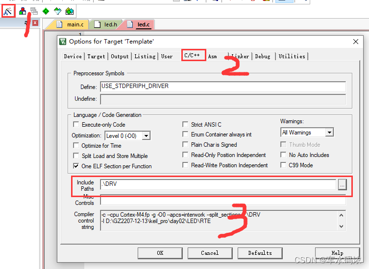
stay keil5 Add source code , The source file should be added to the project directory on the left of the project , The path of the header file is added to the configuration interface C/C++ Of include paths in
——————————————————————————————————————————————————————————————————————————————————————
GPIO Bit segment operation
The operation of registers is usually in binary , Relatively speaking, it is not so convenient ,stm32 Bit segment operation is provided to allow developers to access some bits in the register more conveniently and efficiently . Bit segment operation is convenient for programming , It also improves the running efficiency of the code , If register access is frequent , You can use bit segment operations .
 bit_word_adddr = bit_band_base+(byte_offset*32)+(bit_number*4)
bit_word_adddr Represents the address of the word to be mapped to the target bit in the alias area
bit_band_base Represents the starting address of the alias area
byte_offset Represents the byte number in the bit segment area where the target bit is located
bit_number Bit position representing the target bit (0-7)
——————————————————————————————————————————————————————————————————————————————————————
practice
utilize GPIO Library function configuration PF9,PF10 Pin is output mode , Push pull output , High speed output , No up and down
// Function code

void led_init(void)
{
    GPIO_InitTypeDef GPIO_InitStruct;

    //1. Turn on GPIOE GPIOF The clock of
    RCC_AHB1PeriphClockCmd(RCC_AHB1Periph_GPIOE|RCC_AHB1Periph_GPIOF,ENABLE);

    //2.GPIO initialization  PF9 PF10 PE13 PE14
    GPIO_InitStruct.GPIO_Mode = GPIO_Mode_OUT;// The output mode
    GPIO_InitStruct.GPIO_OType = GPIO_OType_PP;// Push pull output
    GPIO_InitStruct.GPIO_Speed = GPIO_Speed_50MHz;// High speed
    GPIO_InitStruct.GPIO_PuPd = GPIO_PuPd_NOPULL;// No up and down
    GPIO_InitStruct.GPIO_Pin = GPIO_Pin_9|GPIO_Pin_10;//PF9 PF10
    GPIO_Init(GPIOF,&GPIO_InitStruct);

    GPIO_InitStruct.GPIO_Pin = GPIO_Pin_13|GPIO_Pin_14;//PE13 PE14
    GPIO_Init(GPIOE,&GPIO_InitStruct);

    //3.LED Off by default
    GPIO_SetBits(GPIOF,GPIO_Pin_9|GPIO_Pin_10);
    GPIO_SetBits(GPIOE,GPIO_Pin_13|GPIO_Pin_14);
}
边栏推荐
- 二叉树专题--AcWing 3540. 二叉搜索树建树(实用板子 构建二叉搜索树 并输出前、中、后序遍历)
- Binary tree topic -- p1030 [noip2001 popularization group] find the first order
- [ark UI] implementation of the startup page of harmonios ETS
- Creation and use of unified links in Huawei applinking
- 二叉树专题--洛谷 P3884 [JLOI2009]二叉树问题(dfs求二叉树深度 bfs求二叉树宽度 dijkstra求最短路)
- Complement (Mathematical Simulation
- Indexer in C #
- Special topic of binary tree -- acwing 1589 Building binary search tree
- Functional interfaces and method references
- 二叉树专题--洛谷 P1229 遍历问题(乘法原理 已知前、后序遍历求中序遍历个数)
猜你喜欢

Special topic of binary tree -- Logu p1229 traversal problem (the number of traversals in the middle order is calculated when the pre and post order traversals of the multiplication principle are know

Verilog and VHDL signed and unsigned number correlation operations
tidb-dm报警DM_sync_process_exists_with_error排查
ren域名有价值吗?值不值得投资?ren域名的应用范围有哪些?
二叉树专题--AcWing 47. 二叉树中和为某一值的路径(前序遍历)
How to transfer event objects and user-defined parameters simultaneously in Huawei express applications
Win11 arm system configuration Net core environment variable
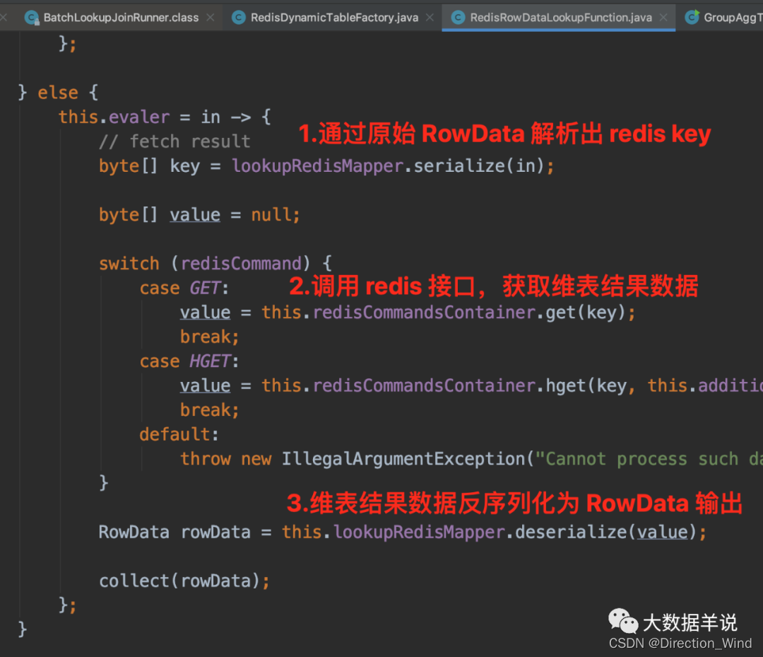
flink二开,实现了个 batch lookup join(附源码)

洛谷 P5536 【XR-3】核心城市(贪心 + 树形 dp 寻找树的中心)
III Chip startup and clock system
随机推荐
JVM garbage collector
How does the whole network display IP ownership?
Luogu p4281 [ahoi2008] emergency gathering / gathering (tree doubling LCA)
Implementation of six singleton modes
通过券商经理的开户二维码开股票账户安全吗?还是去证券公司开户安全?
Resources读取2d纹理 转换为png格式
TIPC Getting Started6
二叉树专题--AcWing 18. 重建二叉树(利用前、中序遍历,构建二叉树)
How to transfer event objects and user-defined parameters simultaneously in Huawei express applications
ros gazebo相关包的安装
一.STM32的开发环境,keil5/MDK5.14安装教程(附下载链接)
VS2019代码中包含中文内容导致的编译错误和打印输出乱码问题
Why does LabVIEW lose precision in floating point numbers
The difference between self and static in PHP in methods
计算序列之和
Gaode draws lines according to the track
洛谷 P3398 仓鼠找 sugar(树上倍增 lca 判断树中两条路径是否相交 结论)
Jinshanyun - 2023 Summer Internship
mmrotate旋转目标检测框架使用记录
js中给数组添加元素的方法有哪些