当前位置:网站首页>DCDC circuit - function of bootstrap capacitor
DCDC circuit - function of bootstrap capacitor
2022-07-05 08:10:00 【Learning notes of hardware Xiaobai】
Recently, when Xiaobai was working on a project , Used one Charge IC. Speaking of Charge IC, Because I just entered the workplace for more than a year . The circuit design of the project is relatively simple , Customers' demand for charging is also very general . So I worked for a year , To really touch Charge IC This species .
Through project learning ,Charge IC In fact, it also uses BUCK Knowledge of circuits , Therefore, the peripheral design of the chip is not very strange . Maybe for previous projects BUCK The reason why the chip peripheral design is relatively simple , What has not been noticed is the bootstrap capacitor , Peripheral pins of the chip BTST And SW An indirect capacitor , It belongs to bootstrap capacitor .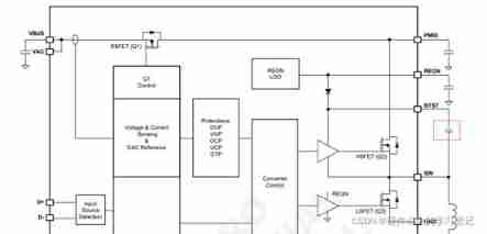
In the past DC-DC In chip , Xiao Bai's pale experience , I have never seen such a design . therefore , In order to figure out every peripheral design that you are not familiar with , I checked the data , Have a simple understanding of this .
Bootstrap capacitors are compared with other ordinary capacitors , No big difference , Mainly used , The voltage difference between the two ends of the capacitor cannot be abrupt Principle . When increasing the voltage at the negative end of the capacitor , The voltage at the positive end will also be raised , The differential pressure remains constant .
Take the illustration in the picture .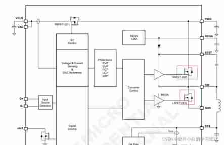
Q2 HSFET(High Side Mosfet) That is, the high side MOS tube Q3 LSFET(Low Side Mosfet) That is, the low side MOS tube .
As the saying goes , Depend on the mountain to eat the mountain , Draw on the water . about Q3 MOS In terms of , Its S Extremely close GND. Therefore, it is very easy to control its conduction and disconnection . Just let the grid voltage be greater than MOS Tubular Vgs(th) that will do . The connection and disconnection of the low side is a good solution , But it's bitter on the high side . Dad doesn't hurt , Mother doesn't love . Its S Pole connection SW, Grid connected BTST. Want to let Q2 Conduction , Must satisfy VBTST>VSW+Vgs(th). VSW It can be regarded as VBUS voltage . For the whole chip , The largest one at the power supply end should be no better than VBUS Still big , So in this case , How can we get more than VBUS To meet VBTST>VSW+Vgs(th) Make the high side MOS The pipe is open .
here , Bootstrap capacitor , Played a great role .
First , At the lower end MOS The pipe is open , Top MOS When the pipe is disconnected .SW Voltage is 0. The capacitance receives from REGN LDO The charge of begins to be charged . Voltage is Vc.
However , At the lower end MOS When the pipe is disconnected , Top MOS When the tube is on . Its S The pole voltage is equal to SW The voltage is approximately VBUS voltage , However, because the voltage difference between the two ends of the capacitor cannot change suddenly ,VBTST Be elevated . Its value is Vc+VBUS Supply power to the grid , Compare the grid voltage with the source voltage , The differential pressure is Vc, For a capacitor voltage , Top MOS The pipe is open .
Due to the existence of diodes , Prevent current backflow ,REGN LDO The output voltage of is always stable and free from VBTST The impact of changes in .
I said that before , The capacitor plays a role in charging , So the capacitance of bootstrap capacitor should be appropriate , Not too small , Too small will cause capacitance voltage difference Vc Too small , Make the high side MOS The tube cannot be connected . Most of the selected values are 10nF-1uF Between .
边栏推荐
- After installing the new version of keil5 or upgrading the JLINK firmware, you will always be prompted about the firmware update
- [popular science] some interesting things that I don't know whether they are useful or not
- L'étude a révélé que le système de service à la clientèle du commerce électronique transfrontalier a ces cinq fonctions!
- Programming knowledge -- basis of C language
- Introduction of air gap, etc
- Ads learning record (lna_atf54143)
- Basic embedded concepts
- Fundamentals of C language
- Some thoughts on extracting perspectives from ealfa and Ebeta
- UEFI development learning 5 - simple use of protocol
猜你喜欢
FIO测试硬盘性能参数和实例详细总结(附源码)

L'étude a révélé que le système de service à la clientèle du commerce électronique transfrontalier a ces cinq fonctions!

Stablq of linked list
Wifi-802.11 negotiation rate table
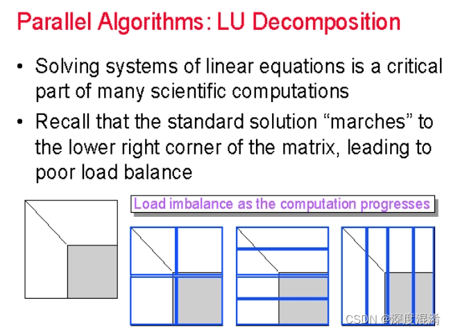
C, Numerical Recipes in C, solution of linear algebraic equations, LU decomposition source program

Win10 shortcut key
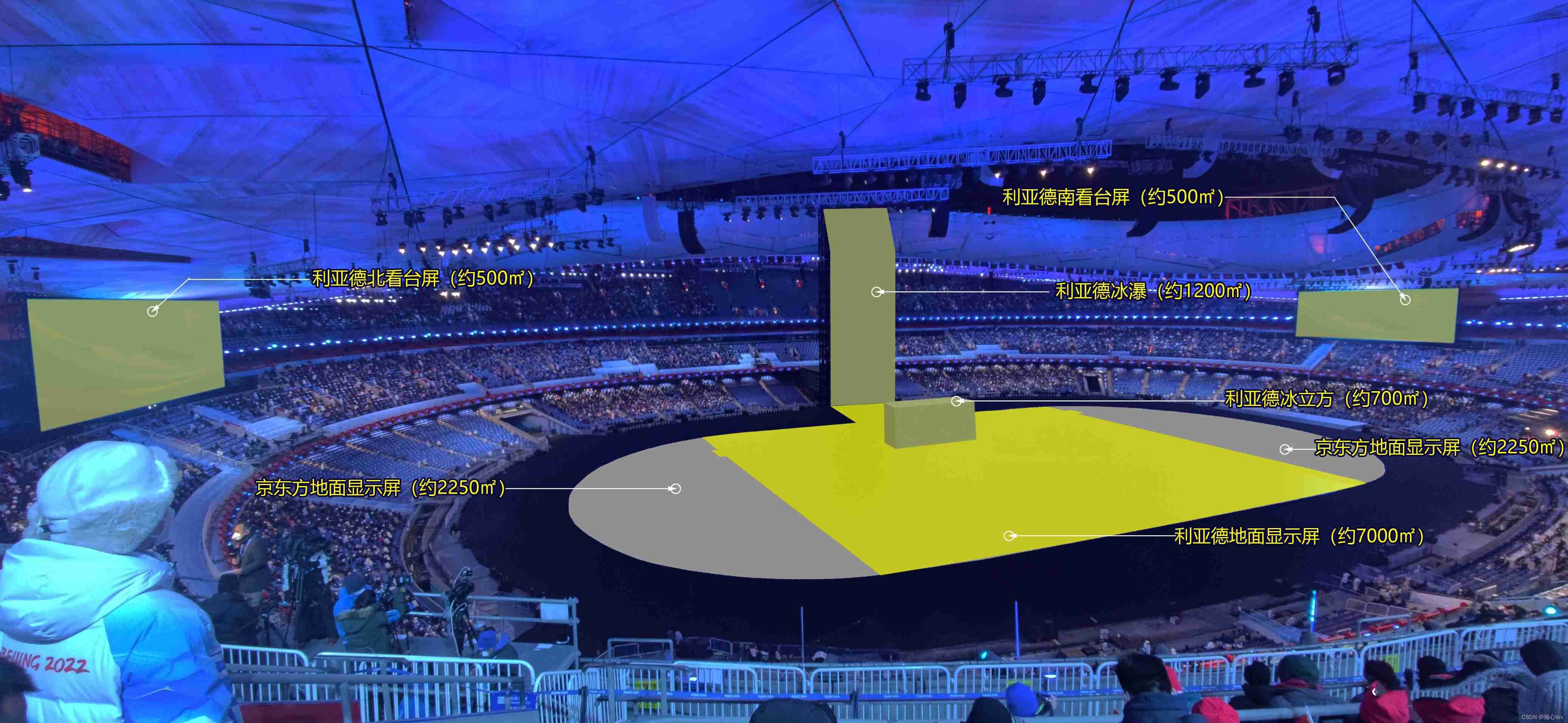
Beijing Winter Olympics opening ceremony display equipment record 3

UEFI development learning 6 - creation of protocol

After installing the new version of keil5 or upgrading the JLINK firmware, you will always be prompted about the firmware update

Arduino uses nrf24l01+ communication
随机推荐
solver. Learning notes of prototxt file parameters
Record the visual shock of the Winter Olympics and the introduction of the screen 2
【云原生 | 从零开始学Kubernetes】三、Kubernetes集群管理工具kubectl
Some thoughts on extracting perspectives from ealfa and Ebeta
Vofa+ software usage record
matlab timeserise
Naming rules for FreeRTOS
[trio basic tutorial 18 from introduction to proficiency] trio motion controller UDP fast exchange data communication
导电滑环磨损快的原因
Correlation based template matching based on Halcon learning [II] find_ ncc_ model_ defocused_ precision. hdev
C language enhancement -- pointer
My-basic application 1: introduction to my-basic parser
[trio basic tutorial 16 from introduction to proficiency] UDP communication test supplement
Detailed explanation of pragma usage
Factors affecting the quality of slip rings in production
[trio basic tutorial 17 from getting started to mastering] set up and connect the trio motion controller and input the activation code
Improve lighting C program
Adaptive filter
[untitled] record the visual shock of the Winter Olympics and the introduction of the display screen
C WinForm [realize the previous and next selection pictures] - practice 7