当前位置:网站首页>Design of NAND flash interface control
Design of NAND flash interface control
2020-11-06 22:06:00 【DISPLAY】
Nand flash yes flash One kind of memory ,Nand flash It adopts nonlinear macro cell mode and provides a cheap and effective solution for the implementation of solid state large capacity memory .NAND FLASH Memory has the advantages of large capacity and fast rewriting speed, which is suitable for the storage of large amounts of data , Therefore, it has been widely used in the industry .NAND The structure can provide extremely high cell density , High storage density , And the speed of writing and erasing is very fast . This article introduces the memory chip supplier Yuxin electronics about NAND Flash Storage structure of and NAND Flash Interface control design of .
NAND Flash Storage structure of
Most of the NAND Flash It's all the same , The only difference is that NAND Flash The basic characteristics of the chip, such as capacity size and read-write speed .
block Block yes NAND Flash The basic of erase operation of / Smallest unit . Page is the basic unit of read and write operations .
Every page , There's another area , It's called the free zone / Redundant areas , And in the Linux In the system ﹐ Generally called OOB(Out Of Band)[2]. This area was originally based on NAND Flash Hardware features of ﹐ Data is relatively error prone when reading and writing ﹐ So in order to ensure the correctness of the data , There must be a corresponding detection and error correction mechanism , This mechanism is called EDC /ECC. So the extra areas are designed ﹐ Check value used to place data .OOB Read and write operations are generally completed along with page operations , When reading and writing a page , Read and write accordingly OOB.OOB Main purpose of : Whether the mark is a bad block ﹐ Storage ECC data ﹐ Store some file system related data .
NAND Flash Interface control design of
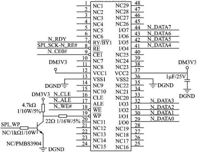
because NAND Flash Only 8 individual I/O Pin , And it's reusable , It can transmit data ﹐ You can also send an address 、 command . Design command latch enable (Command Latch Enable,CLE) And address latch enable ( Ad-dress Latch Enable,ALE), That is to send a CLE( or ALE) command , tell NAND Flash A sound from the controller , The picture to be passed on below 1NAND Flash The control circuit is a command ( Or address ). such NAND Flash Internal ability according to the content of the incoming ﹐ Do the corresponding action . Relative to parallel port NOR Flash Of 48 or 52 One pin , Greatly reduces the number of pins , In this way, the chip is small in size . At the same time, the chip interface is reduced ﹐ The peripheral circuits associated with this chip will be simplified , Avoid cumbersome hardware wiring .
NAND Flash The interface control circuit is shown in the figure 1 Shown
版权声明
本文为[DISPLAY]所创,转载请带上原文链接,感谢
边栏推荐
- ado.net and asp.net The relationship between
- August 14, 2020: what are the execution engines for data tasks?
- [elastic search engine]
- Elasticsearch database | elasticsearch-7.5.0 application construction
- The Interpreter pattern of behavior pattern
- 谷歌浏览器实现视频播放加速功能
- 2020-08-17: how to solve data skew in detail?
- 2020-08-19:TCP是通过什么机制保障可靠性的?
- Js数组-数组的用法全在这里(数组方法的重构、数组的遍历、数组的去重,数组的判断与转换)
- 【涂鸦物联网足迹】物联网基础介绍篇
猜你喜欢

统计项目代码行数

2020 database technology conference helps technology upgrade

【涂鸦物联网足迹】涂鸦云平台全景介绍

Unity performance optimization

Elasticsearch database | elasticsearch-7.5.0 application construction

STM32F030K6T6兼容替换灵动MM32F031K6T6

实验一

2020-08-15: under what circumstances should data tasks be optimized?

The native API of the future trend of the front end: web components

Countdown | 2020 PostgreSQL Asia Conference - agenda arrangement of Chinese sub Forum
随机推荐
Es create a new index database and copy the old index library, practice pro test effective!
The method of local search port number occupation in Windows system
ES6 learning notes (3): teach you to use js object-oriented thinking to realize the function of adding, deleting, modifying and checking tab column
August 18, 2020: introduce Mr process?
An article will introduce you to CSS3 background knowledge
2020-09-09:裸写算法:两个线程轮流打印数字1-100。
jenkins安装部署过程简记
September 9, 2020: naked writing algorithm: two threads print numbers 1-100 in turn.
C and C / C + + mixed programming series 5 - GC collaboration of memory management
谷歌浏览器实现视频播放加速功能
How to manage the authority of database account?
Event monitoring problem
2020-08-19:TCP是通过什么机制保障可靠性的?
递归、回溯算法常用数学基础公式
Method of code refactoring -- Analysis of method refactoring
2020-08-19: what mechanism does TCP ensure reliability?
[elastic search engine]
STM32F030F4P6兼容灵动微MM32F031F4P6
[forward] how to view UserData in Lua
Countdown | 2020 PostgreSQL Asia Conference - agenda arrangement of Chinese sub Forum
