当前位置:网站首页>ADC of stm32
ADC of stm32
2022-07-02 23:10:00 【What's your name】

List of articles
One 、ADC brief introduction
ADC (Analog-Digital Converter) simulation - Numbers converter
ADC The continuous changing analog voltage on the pin can be converted into digital variables stored in memory , Build a bridge from analog circuit to digital circuit .12 position Successive approximation type ADC**,1us Conversion time
Input voltage range ∶0-3.3V, Conversion result range ∶0~4095.18 Input channels , Can be measured 16 Outside and 2 There are two conversion units of internal signal source rule group and injection group
Simulation watchdog Automatically monitor the input voltage range **
12 position ADC Value , The scope of quantification is 0 - 2^12-1 , namely 0-4095. The higher the number of digits . The more refined the quantitative results . The higher the corresponding resolution .
About this simulated watchdog , We can set the threshold . When AD When the value is higher than the upper threshold or lower than the lower threshold , It will apply for interruption , You can perform the corresponding operation in the interrupt function .
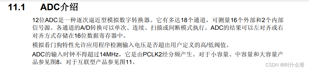
1、 Successive approximation type ADC
STM32 Of ADC The principle of is the same as this , This is ADC0809 The internal structure of 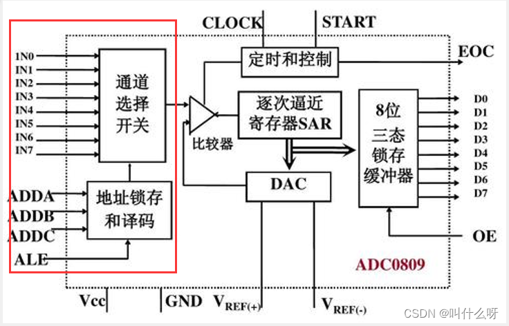
First, select the channel switch . There is a channel selector switch on the left . The number of the selected channel exists below ADDA,ADDB,ADDC in . You want to choose IN0-IN7 Which channel in , Just put the channel number in these three .ALE It is a latch signal , to ALE Set up , The corresponding path switch here above can be automatically dialed .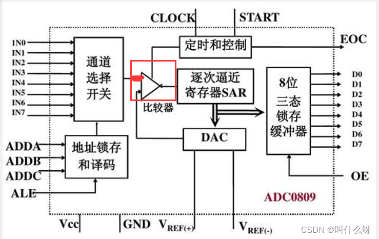
Then came to the upper line of the comparator .
Use the successive approximation method in the comparator to compare one by one
The function of the comparator is to judge the relationship between the two input signal voltages .
The upper line of the comparator is input by an external channel , Unknown encoded voltage .
The lower line of the comparator is a DAC Output , Known encoded voltage .
If DAC The output voltage is relatively small . I will grow DAC data . until DAC The output voltage is equal to the input voltage of the external channel . such DAC The input data is the encoded data of the external voltage .( Here is the input to 8 Bit tristate latch buffer )
And this increase or decrease to adjust DAC The process of data , It's the successive approximation register SAR It's working .
It usually uses dichotomy to find , For example, here is 8 Bit ADC, Namely 0-255. When comparing for the first time , We'll give it to DAC Input 255 Half of . The second comparison . Give it again 128 Half of 64. Just continue to compare . and 128,64,32 Just the bit weight of each bit in binary . in other words , This process of comparison , It is to judge binary from high to low in order 1 yes 0 The process of . The for 8 Bit ADC, Judge from high to low 8 The code of unknown voltage can be found once .12 Bit is judgment 12 Time .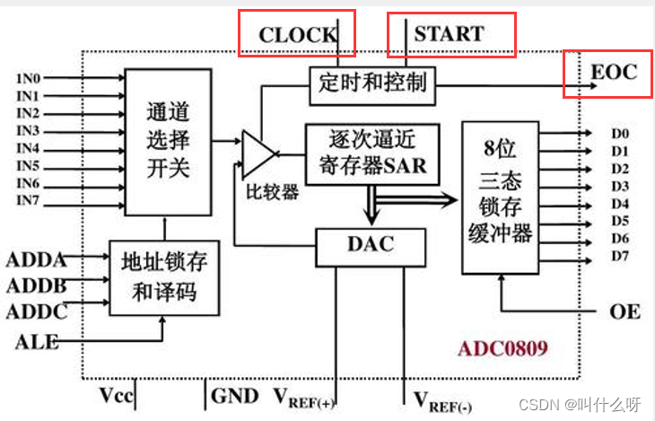
EOC yes End Of Gonvert Conversion end signal
START Is to start the conversion . Give an input pulse , Start conversion .
CLOCK yes ADC The clock .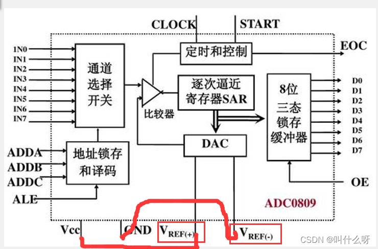
below .VRVF+ and VREF- yes DAC The reference voltage of .
For example, you give a data 255. It's corresponding to 5V still 3.3V Well , It depends on the reference voltage .
This DAC The reference voltage of also determines ADC Input range of , So it's also ADC Reference voltage .
Generally, the positive pole of the reference voltage and VCC It's the same , Will connect . The negative pole of the reference electricity and GND It's the same . Also connected .
2、ADC Block diagram
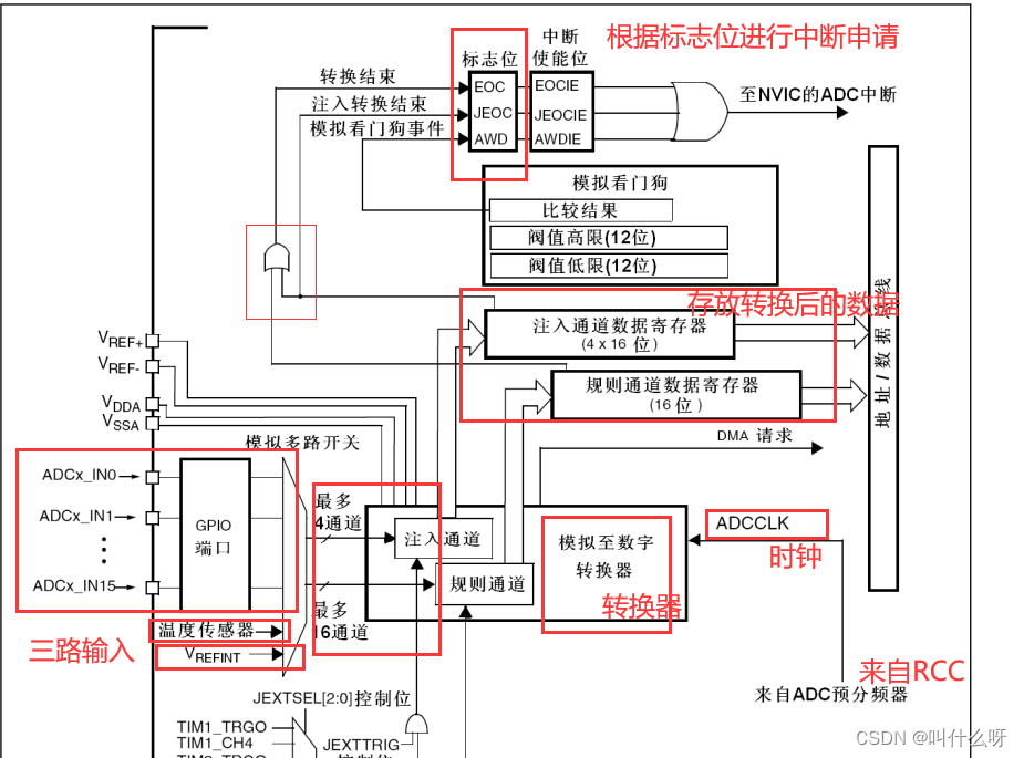
3、ADC The basic structure

On the left is the input channel ,16 individual GPO mouth , Plus two internal channels .
Then enter AD converter
AD There are two groups in the converter , One is the rule group , One is the injection group
Rule groups can be selected at most 16 Channels . The injection group can select at most 4 Channels .
Then the conversion results can be stored in AD In the data register , The rule group has 1 Data registers , The injection group has 4 Data registers .
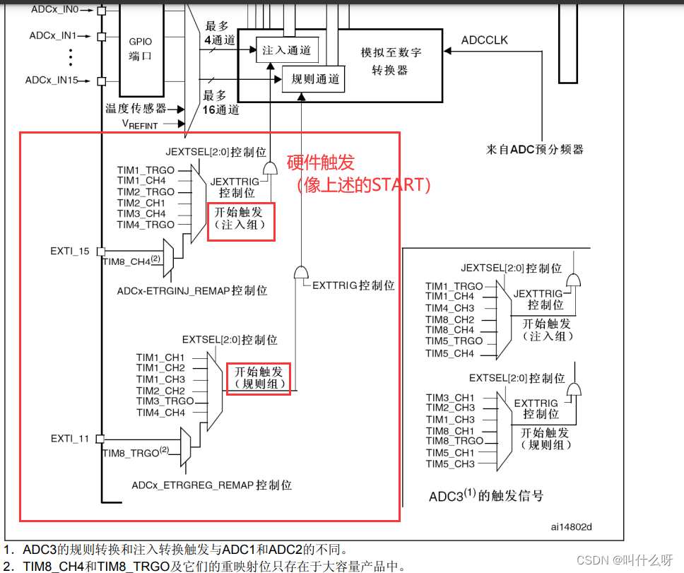
Then here is the trigger control . Provides the... To start the conversion START The signal .
Trigger control can select hardware trigger and software trigger , Hardware trigger mainly comes from timer and external interrupt trigger .
On the right here is from RCC Of ADC The clock CLOCK,ADC The process of successive comparison is driven by this clock
There are three ways to apply for interruption , First of all, there will be EOC The signal , A flag bit will be set . Next is the watchdog , If the threshold is exceeded , Control through interrupt output , image NVIC Application interruption .
4、 Conversion mode


Rule group 
Trigger — Enter the first sequence position ( Choose 1 individual )---- Then the conversion is finished
At this point, a EOC The signal of
If you want to convert, you need to trigger again
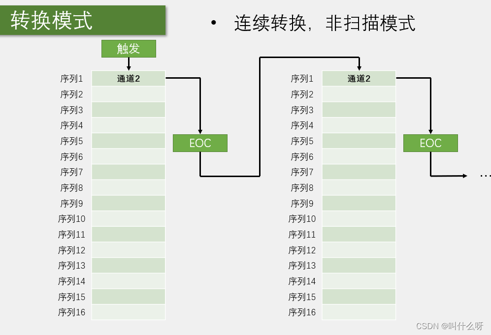
Trigger — Enter the first sequence position ( Choose 1 individual )---- This conversion is completed ----- Generate EOC ----- Do not need to trigger and continue to repeat the above process

This mode is also triggered once
But there are several sequences at a time
So give a number of channels , There are several sequences that can be used , There are several from the sequence 1 Start to row down a few
After each trigger , Just before this 7 individual ( Number of channels ) Conduct AD transformation , And to prevent data coverage , Use it in time DMA Remove the data
that 7 After the conversion of channels , produce EOC The signal , End of conversion .

This is the above process , When triggered, it keeps turning
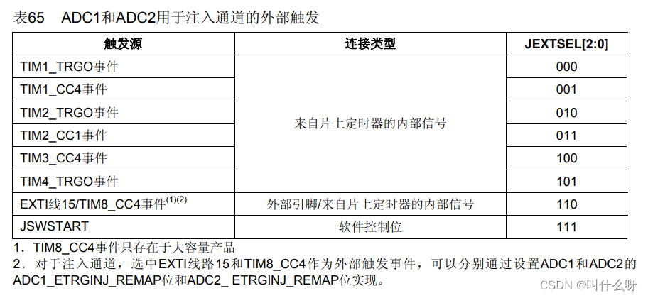
5、 Trigger control

6、 Data alignment

Generally, it is right aligned , Add in front 0.
There are also cases of left alignment
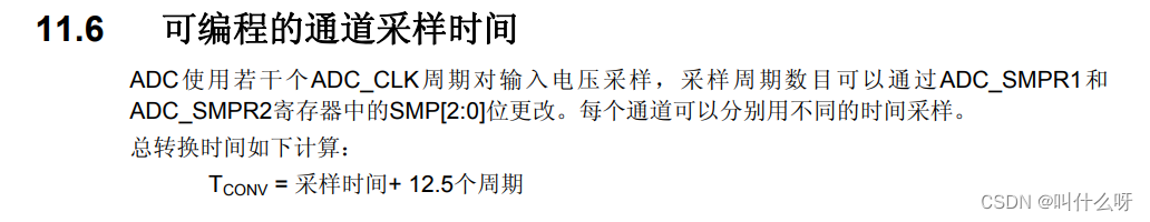
7、 Channel sampling time


8、 calibration
1、ADC There is a built-in self calibration mode . Calibration can greatly reduce the quasi precision error caused by the change of internal capacitor bank . During calibration , An error correction code will be calculated on each capacitor ( Numerical value ), This code is used to eliminate the error on each capacitor in the subsequent conversion .
2、 It is recommended to perform a calibration after each power on .
3、 Before starting calibration ,ADC Must be in power off state for at least two ADC Clock cycle .
Two 、 Code
The board I use is a mini board of punctual atoms
STM32 The model number is STM32F103RCT
There are three ADC
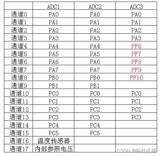
We use it here ADC1 The passage of 1
1、 Some functions


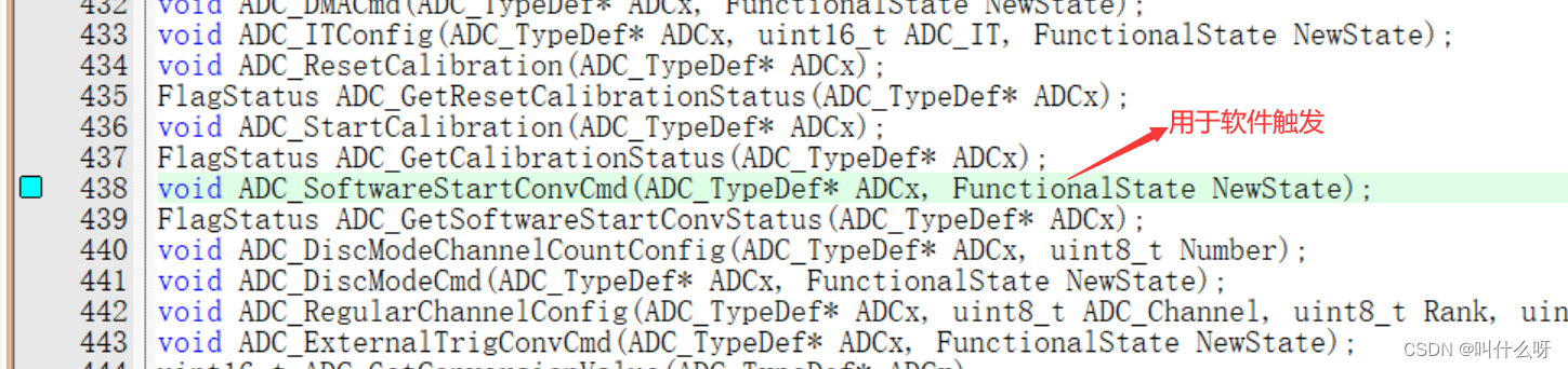


ADC Rule group channel configuration
void ADC_RegularChannelConfig(ADC_TypeDef* ADCx, uint8_t ADC_Channel, uint8_t Rank, uint8_t ADC_SampleTime);
Whether to allow external trigger conversion
void ADC_ExternalTrigInjectedConvCmd(ADC_TypeDef* ADCx, FunctionalState NewState);
Get the conversion value
uint16_t ADC_GetConversionValue(ADC_TypeDef* ADCx);
double ADC Mode read conversion result
uint32_t ADC_GetDualModeConversionValue(void);

2、ADC initialization
#include "stm32f10x.h"

void Adc_Init()
{

	GPIO_InitTypeDef GPIO_InitStructure;
	ADC_InitTypeDef ADC_InitStructure;

	//1、 Turn on the clock ADC1 Clock and GPIOA The clock of
	RCC_APB2PeriphClockCmd(RCC_APB2Periph_ADC1,ENABLE );
	RCC_APB2PeriphClockCmd(RCC_APB2Periph_GPIOA,ENABLE );
	//2、 Configure frequency division , Because the maximum cannot exceed 14MHz 72/6=12
	RCC_ADCCLKConfig(RCC_PCLK2_Div6);   // Set up ADC Division factor 6 72M/6=12,ADC The maximum time cannot exceed 14M
	//3、 To configure GPIOA and ADC Structure  PA1  As an analog channel input pin
	GPIO_InitStructure.GPIO_Pin = GPIO_Pin_1;
	GPIO_InitStructure.GPIO_Mode = GPIO_Mode_AIN;		// Analog input pins
	GPIO_Init(GPIOA, &GPIO_InitStructure);

	ADC_DeInit(ADC1); // Reset ADC1

	ADC_InitStructure.ADC_Mode = ADC_Mode_Independent;	//ADC Working mode :ADC1 and ADC2 Working in independent mode
	ADC_InitStructure.ADC_ScanConvMode = DISABLE;	// Analog to digital conversion works in single channel mode
	ADC_InitStructure.ADC_ContinuousConvMode = DISABLE;	// A / D conversion works in single conversion mode
	ADC_InitStructure.ADC_ExternalTrigConv = ADC_ExternalTrigConv_None;	// The transformation is initiated by software rather than external triggers
	ADC_InitStructure.ADC_DataAlign = ADC_DataAlign_Right;	//ADC Data right alignment
	ADC_InitStructure.ADC_NbrOfChannel = 1;	// In order to change the rules ADC The number of channels
	ADC_Init(ADC1, &ADC_InitStructure);	// according to ADC_InitStruct The parameter specified in ADCx The register of
	//4、 Can make ADC1
	ADC_Cmd(ADC1, ENABLE);
	//5、 Calibrate and wait for the calibration to end
	ADC_ResetCalibration(ADC1);	// Enable reset calibration

	while(ADC_GetResetCalibrationStatus(ADC1));	// Wait for the reset calibration to finish

	ADC_StartCalibration(ADC1);	 // Turn on AD calibration

	while(ADC_GetCalibrationStatus(ADC1));	 // Wait for the calibration to finish

}
About frequency division 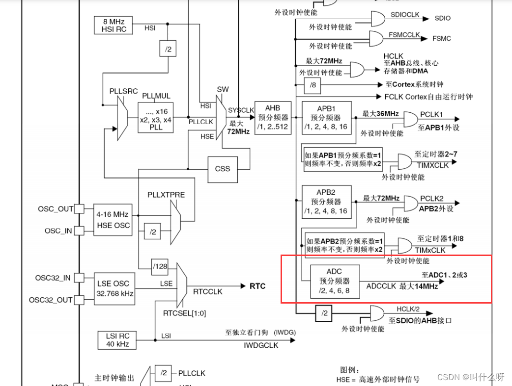

3、 Experimental acquisition PA1 And display
First PA1 yes ADC passageway 1
So in this function ADC_Channel Select as shown in the figure
void ADC_RegularChannelConfig(ADC_TypeDef* ADCx, uint8_t ADC_Channel, uint8_t Rank, uint8_t ADC_SampleTime)

adc.c
#include "stm32f10x.h"

void Adc_Init()
{

	GPIO_InitTypeDef GPIO_InitStructure;
	ADC_InitTypeDef ADC_InitStructure;

	//1、 Turn on the clock ADC1 Clock and GPIOA The clock of
	RCC_APB2PeriphClockCmd(RCC_APB2Periph_ADC1,ENABLE );
	RCC_APB2PeriphClockCmd(RCC_APB2Periph_GPIOA,ENABLE );
	//2、 Configure frequency division , Because the maximum cannot exceed 14MHz 72/6=12
	RCC_ADCCLKConfig(RCC_PCLK2_Div6);   // Set up ADC Division factor 6 72M/6=12,ADC The maximum time cannot exceed 14M
	//3、 To configure GPIOA and ADC Structure  PA1  As an analog channel input pin
	GPIO_InitStructure.GPIO_Pin = GPIO_Pin_1;
	GPIO_InitStructure.GPIO_Mode = GPIO_Mode_AIN;		// Analog input pins
	GPIO_Init(GPIOA, &GPIO_InitStructure);

	ADC_DeInit(ADC1); // Reset ADC1

	ADC_InitStructure.ADC_Mode = ADC_Mode_Independent;	//ADC Working mode :ADC1 and ADC2 Working in independent mode
	ADC_InitStructure.ADC_ScanConvMode = DISABLE;	// Analog to digital conversion works in single channel mode
	ADC_InitStructure.ADC_ContinuousConvMode = DISABLE;	// A / D conversion works in single conversion mode
	ADC_InitStructure.ADC_ExternalTrigConv = ADC_ExternalTrigConv_None;	// The transformation is initiated by software rather than external triggers
	ADC_InitStructure.ADC_DataAlign = ADC_DataAlign_Right;	//ADC Data right alignment
	ADC_InitStructure.ADC_NbrOfChannel = 1;	// In order to change the rules ADC The number of channels
	ADC_Init(ADC1, &ADC_InitStructure);	// according to ADC_InitStruct The parameter specified in ADCx The register of
	//4、 Can make ADC1
	ADC_Cmd(ADC1, ENABLE);
	//5、 Calibrate and wait for the calibration to end
	ADC_ResetCalibration(ADC1);	// Enable reset calibration

	while(ADC_GetResetCalibrationStatus(ADC1));	// Wait for the reset calibration to finish

	ADC_StartCalibration(ADC1);	 // Turn on AD calibration

	while(ADC_GetCalibrationStatus(ADC1));	 // Wait for the calibration to finish

}

uint16_t AD_GetValue(u8 ch)
{

		// Set the specified ADC The rule group channel for , A sequence , Sampling time
	ADC_RegularChannelConfig(ADC1, ch, 1, ADC_SampleTime_239Cycles5 );	//ADC1,ADC passageway , The sampling time is 239.5 cycle

	ADC_SoftwareStartConvCmd(ADC1, ENABLE);		// Enable to designate ADC1 Software conversion start function

	while(!ADC_GetFlagStatus(ADC1, ADC_FLAG_EOC ));// Wait for the conversion to finish

	return ADC_GetConversionValue(ADC1);	// Go back to the last time ADC1 Conversion result of rule group
}

// It is more stable to obtain the average value by obtaining more data
uint16_t Get_Adc_Average(u8 ch,u8 times)
{

	u32 temp_val=0;
	u8 t;
	for(t=0;t<times;t++)
	{

		temp_val+=AD_GetValue(ch);
		delay_ms(5);
	}
	return temp_val/times;
}
main.c
#include "stm32f10x.h"

#include "delay.h"
#include "ADC.h"
#include "lcd.h"


 int main(void)
 {

	float temp;
	u16 adcx;
	delay_init();	    	 // Delay function initialization
	LCD_Init();
	Adc_Init();
	 	LCD_ShowString(10,70,200,16,16,"AD_GetValue");
		LCD_ShowString(10,100,200,16,16,"AD_Average");
		LCD_ShowString(10,150,200,16,16,"ADC_CH1_VOL:0.000V");
  while(1)
	{

		LCD_ShowxNum(110,70,AD_GetValue(ADC_Channel_1),4,16,0);
		LCD_ShowxNum(110,100,Get_Adc_Average(ADC_Channel_1,10),4,16,0);

		adcx=Get_Adc_Average(ADC_Channel_1,10);
		temp=(float)adcx*(3.3/4096);
		adcx=temp;
		LCD_ShowxNum(106,150,adcx,1,16,0);// Show integers
		temp-=adcx;
		temp*=1000;
		LCD_ShowxNum(122,150,temp,3,16,0X80); // Display decimal
	}
 }
Pick up 3.3v And then GND And if not, it's floating , The level is unstable and keeps changing 


边栏推荐
- 20220524_数据库过程_语句留档
- MySQL reset password, forget password, reset root password, reset MySQL password
- 剑指 Offer II 099. 最小路径之和-双百代码
- 泛型与反射,看这篇就够了
- Editor Caton
- [羊城杯2020]easyphp
- Freshman learning sharing
- 创新实力再获认可!腾讯安全MSS获2022年度云原生安全守护先锋
- [chestnut sugar GIS] ArcScene - how to make elevation map with height
- Configuration clic droit pour choisir d'ouvrir le fichier avec vs Code
猜你喜欢

Motivation du Protocole de chiffrement avancé AES

【喜欢的诗词】好了歌
C#中Linq用法汇集
LeetCode 968. 监控二叉树

Strictly abide by the construction period and ensure the quality, this AI data annotation company has done it!
实现BottomNavigationView和Navigation联动
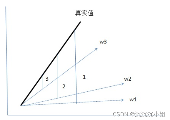
Loss function~

力扣刷题(2022-6-28)
Set right click to select vs code to open the file
![[chestnut sugar GIS] ArcScene - how to make elevation map with height](/img/91/f3df0a7633263c6264cb5c27eb149f.png)
[chestnut sugar GIS] ArcScene - how to make elevation map with height
随机推荐
程序员版本的八荣八耻~
Detailed explanation and application of merging and sorting
解决Chrome浏览器和Edeg浏览器主页被篡改的方法
Lambda expression: an article takes you through
設置單擊右鍵可以選擇用VS Code打開文件
Lambda表达式:一篇文章带你通透
Jerry's charge unplugged, unable to touch the boot [chapter]
Start from the bottom structure to learn the customization and testing of FPGA --- Xilinx ROM IP
AES高級加密協議的動機闡述
Xshell configuration xforward forwarding Firefox browser
LeetCode 968. 监控二叉树
[Solved] Splunk: Cannot get username when all users are selected“
20220527_ Database process_ Statement retention
Loss function~
Construction of Hisilicon 3559 universal platform: draw a frame on the captured YUV image
最小生成树 Minimum Spanning Tree
MySQL查询附近的数据.并按距离进行排序.
[npuctf2020]ezlogin XPath injection
Doorplate making C language
SQL advanced syntax