当前位置:网站首页>How to improve the thermal management in PCB design with the effective placement of thermal through holes?
How to improve the thermal management in PCB design with the effective placement of thermal through holes?
2022-07-05 18:01:00 【IDC Technology】
In the design PCB when , There are many cases where we need some components ( For example, linear regulator ) Dissipate heat . in the majority of cases , These devices are general-purpose through-hole components , Therefore, the radiator effectively distributes heat in the aluminum area , And keep the equipment under cold environmental conditions . however , If we talk about anything SMD equipment , Radiators are not available , And most of the time , We have to use Copper clad Technology Create enough radiators on the copper layer . Now? , This may be an effective solution , But it's better to use it alone PCB The aluminum radiator of the component in is effective .
Designers have two choices :
- Use as much copper as possible inside the circuit board .
- Use a separate radiator to compensate for additional heat dissipation .
When possible , Many designers choose the first option , Because it is more cost-effective ( If carefully designed and extra PCB Space will not affect PCB The size of the ) And will not affect the manufacturing process , Because aluminum radiators need screws , Hot sealant , This is extra manufacturing work . Now? , Limited space PCB You can use the top and bottom layers , And connect the two layers to distribute heat , And it can be used as copper in a larger area . We are all familiar with vias . Via yes PCB Connecting holes connecting different copper layers in . These same vias can be placed under the thermal pad of surface mount devices , If it is a multilayer board , This allows heat to be transferred from the top layer to the bottom or other layers . These are called Hot through hole on the assembly pad Sure Reduce heat dissipation .
Placement of hot through holes
The location and size of the cooling holes vary greatly , It depends on the type of component 、 Different rules and expertise .
But a main rule is to use a hot through hole directly below the heating element as close to the heating source as possible . However , When the heat dissipation is not ideal , Regardless of the position of the component pad , The hot through hole can also be placed on the periphery of the component . under these circumstances , The rules also remain unchanged , Place the through-hole as close to the periphery of the component as possible .
Thermal conductivity of different materials
thermal conductivity Is a key factor , Used to determine how much heat the material can absorb . The following table allows you to understand the thermal conductivity of different materials . With the help of this table , We can make rules on how to manage through holes .
See the table below :
material | Thermal conductivity (W/mK) |
|---|---|
copper | 388 |
Lead frame | 277 |
aluminum | 205 |
silicon | 145 |
SnAgCu Solder | 57.3 |
63Sn37Pb material | 50 |
DA Epoxy ( Chip bonding epoxy ) | 2.4 |
Molding compound | 0.7 |
FR4 Circuit board | 0.35 |
therefore , It can be seen from the above table that , The thermal conductivity of aluminum is worse than that of copper . however , Because the area of aluminum radiator is larger , And it has a more effective cooling effect on the heating equipment . however , As we can see , If copper is used effectively , It can emit more heat than aluminum with the same area .
The effective placement of thermal vias is in IC Correctly use vias or conductive heating element pads as heat transfer methods , Heat is distributed between layers of copper , Then through free air , Heat dissipation begins to use convection to transfer in the air . It is suggested that the inner diameter of the hot through hole should be smaller , for example - about 0.35 mm. If the aperture is large , Incorrect tin absorption may occur during reflow soldering , So you need to be extra careful . However , If you need a larger diameter , Hot pads may help make up for this .
Key points to remember when placing heat dissipation vias
There are few matters needing attention in the process of hot through hole design , It mainly includes the following points :
1. The exposed pad is designed in such a way that the heat will be transferred directly from the shell to the copper area . The effect of solder as a heat sink is not significant , Because it's thin , And the conductivity of solder is very poor .
The figure above shows U1 Hot vias on exposed pads .
2. For bare pad packaging , The maximum heat dissipation occurs from the through hole to PCB Bottom , And then send it into the air . therefore , Having a large bottom layer will also reduce the heat dissipation of cross component packaging .
3. Separating heating elements and using thermal vias to distribute heat helps to distribute heat evenly on other packages .
4. The cooling hole is DFN、QFN The only heat dissipation source on the package , Because of pin assignment , There is no maximum space for copper cladding on the top . therefore , Use bottom copper , The only way to increase thermal conductivity is to use thermal vias .
U5 and IC2 Use hot through holes .IC2 Use QFN Flatpack , Among them, hot through hole is the only possibility , Because of the distribution of component pads , This does not include the larger copper area on the welding layer .
5. The effective copper area of the hot through-hole connection equipment will be the maximum copper length that uses the hot through-hole to directly connect with the component package ( It has nothing to do with the welding layer ).
6. The thickness of the copper plane is also the cause of heat conduction .2Oz Copper ratio 1.0 Oz or 0.5Oz Copper provides better heat resistance .
therefore , This is the standard practice of using hot through holes . I hope this article is helpful to many people who need to carefully consider the design process and placement process of heat dissipation equipment .
This paper is written by IC Mr. Wang www.mrchip.cn Edit and organize , Do not reprint . Picture source network , If there is infringement, please contact to delete .
边栏推荐
猜你喜欢

EPM related

What are the requirements for PMP certification? How much is it?

Nanjing University: Discussion on the training program of digital talents in the new era
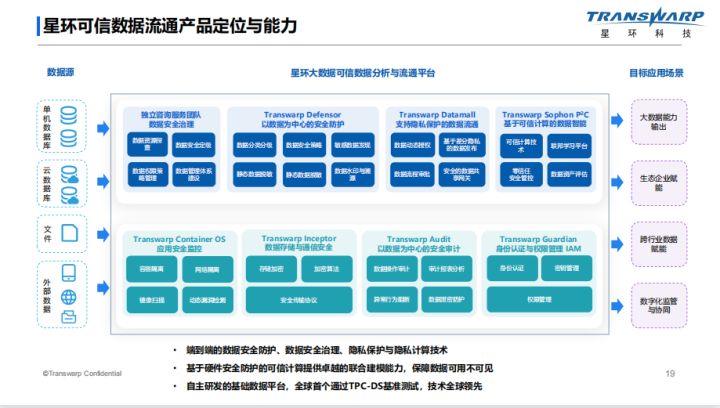
Privacy computing helps secure data circulation and sharing
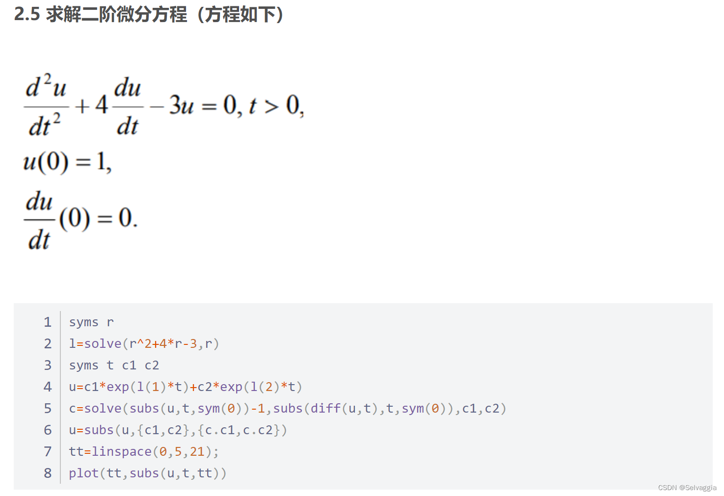
MATLAB查阅
南京大学:新时代数字化人才培养方案探讨
Sophon Base 3.1 推出MLOps功能,为企业AI能力运营插上翅膀

Zabbix
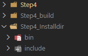
Cmake tutorial Step4 (installation and testing)

Ten capabilities that cyber threat analysts should have
随机推荐
多线程(一) 进程与线程
To solve the stubborn problem of Lake + warehouse hybrid architecture, xinghuan Technology launched an independent and controllable cloud native Lake warehouse integrated platform
tkinter窗口预加载
Leetcode daily practice: rotating arrays
使用QT遍历Json文档及搜索子对象
[BeanShell] there are many ways to write data locally
Sophon CE社区版上线,免费Get轻量易用、高效智能的数据分析工具
从XML架构生成类
LeetCode每日一题:合并两个有序数组
通过SOCKS代理渗透整个内网
MATLAB中print函数使用
访问数据库使用redis作为mysql的缓存(redis和mysql结合)
Compared with the loss of Wenxin, the performance is improved a lot
外盘黄金哪个平台正规安全,怎么辨别?
Ten capabilities that cyber threat analysts should have
怎么选择外盘期货平台最正规安全?
星环科技数据安全管理平台 Defensor重磅发布
Simple query cost estimation
What are the requirements for PMP certification? How much is it?
RSE2020/云检测:基于弱监督深度学习的高分辨率遥感图像精确云检测